SLVS642F April 2006 – January 2024 TPS5420
PRODUCTION DATA
- 1
- 1Features
- 2Applications
- 3Description
- 4Electrostatic Discharge Caution
- 5Ordering Information
- 6Pin Assignments
- 7Specifications
-
8Application Information
- 8.1 Functional Block Diagram
- 8.2
Detailed Description
- 8.2.1 Oscillator Frequency
- 8.2.2 Voltage Reference
- 8.2.3 Enable (ENA) and Internal Slow Start
- 8.2.4 Undervoltage Lockout (UVLO)
- 8.2.5 Boost Capacitor (BOOT)
- 8.2.6 Output Feedback (VSENSE)
- 8.2.7 Internal Compensation
- 8.2.8 Voltage Feed Forward
- 8.2.9 Pulse-Width-Modulation (PWM) Control
- 8.2.10 Overcurrent Limiting
- 8.2.11 Overvoltage Protection
- 8.2.12 Thermal Shutdown
- 8.2.13 PCB Layout
- 8.2.14 Application Circuits
- 8.2.15
Design Procedure
- 8.2.15.1 Design Parameters
- 8.2.15.2 Switching Frequency
- 8.2.15.3 Input Capacitors
- 8.2.15.4 Output Filter Components
- 8.2.15.5 Output Voltage Setpoint
- 8.2.15.6 Boot Capacitor
- 8.2.15.7 Catch Diode
- 8.2.15.8 Additional Circuits
- 8.2.15.9 Circuit Using Ceramic Output Filter Capacitors
- 8.2.15.10 Output Filter Component Selection
- 8.2.15.11 External Compensation Network
- 8.3 Advanced Information
- 8.4 Performance Graphs
- 9Revision History
Package Options
Mechanical Data (Package|Pins)
- D|8
Thermal pad, mechanical data (Package|Pins)
Orderable Information
7.6 Typical Characteristics
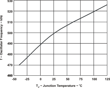 Figure 7-1 OSCILLATOR FREQUENCY vs
JUNCTION TEMPERATURE
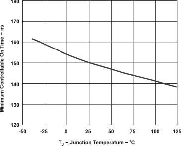 Figure 7-3 MINIMUM CONTROLLABLE ON TIME vsJUNCTION TEMPERATURE
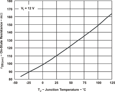 Figure 7-5 ON STATE RESISTANCE vsJUNCTION TEMPERATURE
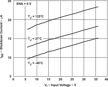 Figure 7-7 SHUTDOWN QUIESCENT CURRENT vs INPUT VOLTAGE
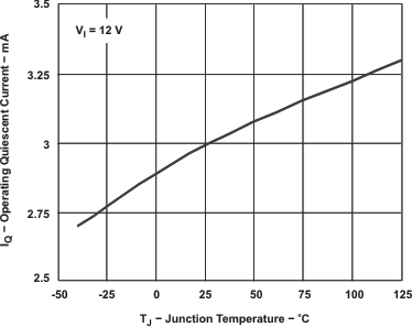 Figure 7-2 OPERATING QUIESCENT CURRENT vsJUNCTION TEMPERATURE
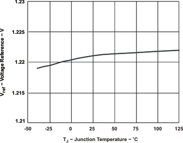 Figure 7-4 VOLTAGE REFERENCE vsJUNCTION TEMPERATURE
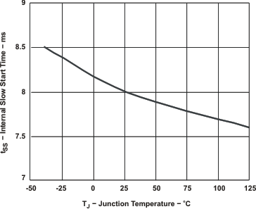 Figure 7-6 INTERNAL SLOW START TIME vsJUNCTION TEMPERATURE
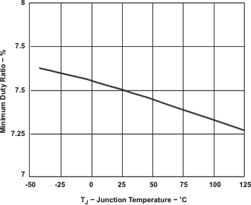 Figure 7-8 MINIMUM CONTROLLABLE DUTY RATIO vs JUNCTION TEMPERATURE