SLUSCO8B November   2016  – June 2018 TPS54200 , TPS54201

PRODUCTION DATA.  

  1. Features
  2. Applications
  3. Description
    1.     Device Images
      1.      Simplified Schematic
      2.      Excellent Deep Dimming in ADIM
  4. Revision History
  5. Description (continued)
  6. Pin Configuration and Functions
    1.     Pin Functions
  7. Specifications
    1. 7.1 Absolute Maximum Ratings
    2. 7.2 ESD Ratings
    3. 7.3 Recommended Operating Conditions
    4. 7.4 Thermal Information
    5. 7.5 Electrical Characteristics
    6. 7.6 Timing Requirements
    7. 7.7 Switching Characteristics
    8. 7.8 Typical Characteristics
  8. Detailed Description
    1. 8.1 Overview
    2. 8.2 Functional Block Diagram
    3. 8.3 Feature Description
      1. 8.3.1  Fixed-Frequency PWM Control
      2. 8.3.2  Error Amplifier
      3. 8.3.3  Slope Compensation and Output Current
      4. 8.3.4  Input Undervoltage Lockout
      5. 8.3.5  Voltage Reference
      6. 8.3.6  Setting LED Current
      7. 8.3.7  Internal Soft Start
      8. 8.3.8  Bootstrap Voltage (BOOT)
      9. 8.3.9  Overcurrent Protection
        1. 8.3.9.1 High-Side MOSFET Overcurrent Protection
        2. 8.3.9.2 Low-Side MOSFET Overcurrent Protection
        3. 8.3.9.3 Low-Side MOSFET Reverse Overcurrent Protection
      10. 8.3.10 Fault Protection
        1. 8.3.10.1 LED-Open Protection
        2. 8.3.10.2 LED Short Protection
        3. 8.3.10.3 Sense-Resistor Short Protection
        4. 8.3.10.4 Sense-Resistor Open Protection
        5. 8.3.10.5 Overvoltage Protection
        6. 8.3.10.6 Thermal Shutdown
    4. 8.4 Device Functional Modes
      1. 8.4.1 Enable and Disable Device
      2. 8.4.2 Mode Detection
      3. 8.4.3 Analog Dimming Mode Operation
      4. 8.4.4 PWM Dimming-Mode Operation
  9. Application and Implementation
    1. 9.1 Application Information
    2. 9.2 Typical Application
      1. 9.2.1 TPS5420x 12-V Input, 1.5-A, 3-Piece IR LED Driver With Analog Dimming
        1. 9.2.1.1 Design Requirements
        2. 9.2.1.2 Detailed Design Procedure
          1. 9.2.1.2.1 Inductor Selection
          2. 9.2.1.2.2 Input Capacitor Selection
          3. 9.2.1.2.3 Output Capacitor Selection
          4. 9.2.1.2.4 FB Pin RC Filter Selection
          5. 9.2.1.2.5 Sense Resistor Selection
        3. 9.2.1.3 Application Curves
      2. 9.2.2 TPS5420x 24-V Input, 1-A, 4-Piece WLED Driver With PWM Dimming
        1. 9.2.2.1 Design Requirements
        2. 9.2.2.2 Detailed Design Procedure
          1. 9.2.2.2.1 Inductor Selection
          2. 9.2.2.2.2 Input Capacitor Selection
          3. 9.2.2.2.3 Output Capacitor Selection
          4. 9.2.2.2.4 FB Pin RC Filter Selection
          5. 9.2.2.2.5 Sense Resistor Selection
        3. 9.2.2.3 Application Curves
  10. 10Power Supply Recommendations
  11. 11Layout
    1. 11.1 Layout Guidelines
    2. 11.2 Layout Example
  12. 12Device and Documentation Support
    1. 12.1 Device Support
      1. 12.1.1 Third-Party Products Disclaimer
    2. 12.2 Documentation Support
      1. 12.2.1 Related Links
    3. 12.3 Receiving Notification of Documentation Updates
    4. 12.4 Community Resources
    5. 12.5 Trademarks
    6. 12.6 Electrostatic Discharge Caution
    7. 12.7 Glossary
  13. 13Mechanical, Packaging, and Orderable Information

Package Options

Mechanical Data (Package|Pins)
Thermal pad, mechanical data (Package|Pins)
Orderable Information

Analog Dimming Mode Operation

Once the analog dimming mode is chosen, the internal voltage reference for the FB pin is approximately 200 mV at full scale, and proportional to the PWM duty cycle as shown in Figure 16. LED current is continuous in this mode, and the current magnitude can be adjusted by changing PWM duty cycle, see Figure 18. Because the internal voltage reference is filtered from the PWM signal, a too-low PWM frequency may cause excessive ripple at the voltage reference. To minimize this ripple, the suggested PWM signal frequency is 10 kHz or higher, such as 50 kHz.
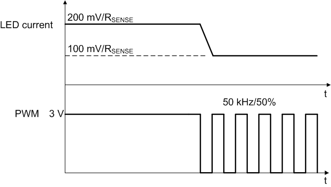
TPS54200 TPS54201 dimop_lusco8.gifFigure 18. Analog Dimming Operation

A comparator with 400-mV hysteresis is used to generate the internal PWM signal, see Figure 17. This internal PWM duty cycle determines the voltage reference. To make sure the PWM pin signal is correctly identified, the high level of the PWM signal should be higher than 1 V, and the low level should be lower than 0.6 V. Figure 19 shows the relationship between the external PWM and internal PWM signals.