SLUSCO8B November   2016  – June 2018 TPS54200 , TPS54201

PRODUCTION DATA.  

  1. Features
  2. Applications
  3. Description
    1.     Device Images
      1.      Simplified Schematic
      2.      Excellent Deep Dimming in ADIM
  4. Revision History
  5. Description (continued)
  6. Pin Configuration and Functions
    1.     Pin Functions
  7. Specifications
    1. 7.1 Absolute Maximum Ratings
    2. 7.2 ESD Ratings
    3. 7.3 Recommended Operating Conditions
    4. 7.4 Thermal Information
    5. 7.5 Electrical Characteristics
    6. 7.6 Timing Requirements
    7. 7.7 Switching Characteristics
    8. 7.8 Typical Characteristics
  8. Detailed Description
    1. 8.1 Overview
    2. 8.2 Functional Block Diagram
    3. 8.3 Feature Description
      1. 8.3.1  Fixed-Frequency PWM Control
      2. 8.3.2  Error Amplifier
      3. 8.3.3  Slope Compensation and Output Current
      4. 8.3.4  Input Undervoltage Lockout
      5. 8.3.5  Voltage Reference
      6. 8.3.6  Setting LED Current
      7. 8.3.7  Internal Soft Start
      8. 8.3.8  Bootstrap Voltage (BOOT)
      9. 8.3.9  Overcurrent Protection
        1. 8.3.9.1 High-Side MOSFET Overcurrent Protection
        2. 8.3.9.2 Low-Side MOSFET Overcurrent Protection
        3. 8.3.9.3 Low-Side MOSFET Reverse Overcurrent Protection
      10. 8.3.10 Fault Protection
        1. 8.3.10.1 LED-Open Protection
        2. 8.3.10.2 LED Short Protection
        3. 8.3.10.3 Sense-Resistor Short Protection
        4. 8.3.10.4 Sense-Resistor Open Protection
        5. 8.3.10.5 Overvoltage Protection
        6. 8.3.10.6 Thermal Shutdown
    4. 8.4 Device Functional Modes
      1. 8.4.1 Enable and Disable Device
      2. 8.4.2 Mode Detection
      3. 8.4.3 Analog Dimming Mode Operation
      4. 8.4.4 PWM Dimming-Mode Operation
  9. Application and Implementation
    1. 9.1 Application Information
    2. 9.2 Typical Application
      1. 9.2.1 TPS5420x 12-V Input, 1.5-A, 3-Piece IR LED Driver With Analog Dimming
        1. 9.2.1.1 Design Requirements
        2. 9.2.1.2 Detailed Design Procedure
          1. 9.2.1.2.1 Inductor Selection
          2. 9.2.1.2.2 Input Capacitor Selection
          3. 9.2.1.2.3 Output Capacitor Selection
          4. 9.2.1.2.4 FB Pin RC Filter Selection
          5. 9.2.1.2.5 Sense Resistor Selection
        3. 9.2.1.3 Application Curves
      2. 9.2.2 TPS5420x 24-V Input, 1-A, 4-Piece WLED Driver With PWM Dimming
        1. 9.2.2.1 Design Requirements
        2. 9.2.2.2 Detailed Design Procedure
          1. 9.2.2.2.1 Inductor Selection
          2. 9.2.2.2.2 Input Capacitor Selection
          3. 9.2.2.2.3 Output Capacitor Selection
          4. 9.2.2.2.4 FB Pin RC Filter Selection
          5. 9.2.2.2.5 Sense Resistor Selection
        3. 9.2.2.3 Application Curves
  10. 10Power Supply Recommendations
  11. 11Layout
    1. 11.1 Layout Guidelines
    2. 11.2 Layout Example
  12. 12Device and Documentation Support
    1. 12.1 Device Support
      1. 12.1.1 Third-Party Products Disclaimer
    2. 12.2 Documentation Support
      1. 12.2.1 Related Links
    3. 12.3 Receiving Notification of Documentation Updates
    4. 12.4 Community Resources
    5. 12.5 Trademarks
    6. 12.6 Electrostatic Discharge Caution
    7. 12.7 Glossary
  13. 13Mechanical, Packaging, and Orderable Information

Package Options

Mechanical Data (Package|Pins)
Thermal pad, mechanical data (Package|Pins)
Orderable Information

Voltage Reference

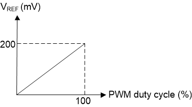
The voltage reference system produces a precise ±2.5% voltage reference over temperature by scaling the output of a temperature-stable band-gap circuit when the PWM duty cycle is 100%. In PWM dimming mode, the voltage reference, VREF, is fixed at 100 mV. In analog dimming mode, VREF, is proportional to the duty cycle of PWM as shown in Figure 16.
TPS54200 TPS54201 voltref_lusco8.gifFigure 16. VREF vs PWM Duty Cycle in Analog Dimming Mode