SLVS996D September 2009 – September 2015 TPS54262-Q1
PRODUCTION DATA.
- 1 Features
- 2 Applications
- 3 Description
- 4 Revision History
- 5 Pin Configuration and Functions
- 6 Specifications
-
7 Detailed Description
- 7.1 Overview
- 7.2 Functional Block Diagram
- 7.3
Feature Description
- 7.3.1 Unregulated Input Voltage
- 7.3.2 Regulated Output Voltage
- 7.3.3 Regulation and Feedback Voltage
- 7.3.4 Enable and Shutdown
- 7.3.5 Soft Start
- 7.3.6 Oscillator Frequency
- 7.3.7 Slew Rate Control
- 7.3.8 Reset
- 7.3.9 Reset Delay
- 7.3.10 Reset Threshold and Undervoltage Threshold
- 7.3.11 Overvoltage Supervisor
- 7.3.12 Noise Filter on RST_TH and OV_TH Terminals
- 7.3.13 Boot Capacitor
- 7.3.14 Short Circuit Protection
- 7.3.15 Overcurrent Protection
- 7.3.16 Internal Undervoltage Lockout (UVLO)
- 7.3.17 Thermal Shutdown (TSD)
- 7.3.18 Loop Control Frequency Compensation - Type 3
- 7.4 Device Functional Modes
-
8 Application and Implementation
- 8.1 Application Information
- 8.2
Typical Application
- 8.2.1 Design Requirements
- 8.2.2
Detailed Design Procedure
- 8.2.2.1
Component Selection
- 8.2.2.1.1 Input Capacitors (C1, C11)
- 8.2.2.1.2 Output Capacitor (C4, C12)
- 8.2.2.1.3 Soft-Start Capacitor (C6)
- 8.2.2.1.4 Bootstrap Capacitor (C3)
- 8.2.2.1.5 Power-On Reset Delay (PORdly) Capacitor (C2)
- 8.2.2.1.6 Output Inductor (L1)
- 8.2.2.1.7 Flyback Schottky Diode (D2)
- 8.2.2.1.8 Resistor to Set Slew Rate (R7)
- 8.2.2.1.9 Resistor to Select Switching Frequency (R8)
- 8.2.2.1.10 Resistors to Select Output Voltage (R4, R5)
- 8.2.2.1.11 Resistors to Set Undervoltage, Overvoltage, and Reset Thresholds (R1, R2, R3)
- 8.2.2.1.12 Low-Power Mode (LPM) Threshold
- 8.2.2.1.13 Enable Pin Pull-Up Resistor (R11) and Voltage Divider Resistor (R10)
- 8.2.2.1.14 Pull-Up Resistor (R12) at RST Pin
- 8.2.2.1.15 Type 3 Compensation Components (R5, R6, R9, C5, C7, C8)
- 8.2.2.1.16 Noise Filter on RST_TH and OV_TH Terminals (C9, C10)
- 8.2.2.2
Design Example 1
- 8.2.2.2.1 Calculate the Switching Frequency (fsw)
- 8.2.2.2.2 Calculate the Ripple Current (IRipple)
- 8.2.2.2.3 Calculate the Inductor Value (L1)
- 8.2.2.2.4 Calculate the Output Capacitor and ESR (C4)
- 8.2.2.2.5 Calculate the Feedback Resistors (R4, R5)
- 8.2.2.2.6 Calculate Type 3 Compensation Components
- 8.2.2.2.7 Calculate Soft-Start Capacitor (C6)
- 8.2.2.2.8 Calculate Bootstrap Capacitor (C3)
- 8.2.2.2.9 Calculate Power-On Reset Delay Capacitor (C2)
- 8.2.2.2.10 Calculate Input Capacitor (C1, C11)
- 8.2.2.2.11 Calculate Resistors to Control Slew Rate (R7)
- 8.2.2.2.12 Resistors to Select Undervoltage, Overvoltage and Reset Threshold Values (R1, R2, R3)
- 8.2.2.2.13 Diode D1 and D2 Selection
- 8.2.2.2.14 Noise Filter on RST_TH and OV_TH Terminals (C9 and C10)
- 8.2.2.2.15 Power Budget and Temperature Estimation
- 8.2.2.3
Design Example 2
- 8.2.2.3.1 Calculate the Switching Frequency (fsw)
- 8.2.2.3.2 Calculate the Ripple Current (IRipple)
- 8.2.2.3.3 Calculate the Inductor Value (L1)
- 8.2.2.3.4 Calculate the Output Capacitor and ESR (C4, C12)
- 8.2.2.3.5 Calculate the Feedback Resistors (R4, R5)
- 8.2.2.3.6 Calculate Type 3 Compensation Components
- 8.2.2.3.7 Calculate Soft-Start Capacitor (C6)
- 8.2.2.3.8 Calculate Bootstrap Capacitor (C3)
- 8.2.2.3.9 Calculate Power-On Reset Delay Capacitor (C2)
- 8.2.2.3.10 Calculate Input Capacitor (C1, C11)
- 8.2.2.3.11 Calculate Resistors to Control Slew Rate (R7)
- 8.2.2.3.12 Resistors to Select Undervoltage, Overvoltage and Reset Threshold Values (R1, R2, R3)
- 8.2.2.3.13 Diode D1 and D2 Selection
- 8.2.2.3.14 Noise Filter on RST_TH and OV_TH Terminals (C9 and C10)
- 8.2.2.3.15 Power Budget and Temperature Estimation
- 8.2.2.1
Component Selection
- 8.2.3 Application Curves
- 9 Power Supply Recommendations
- 10Layout
- 11Device and Documentation Support
- 12Mechanical, Packaging, and Orderable Information
Package Options
Mechanical Data (Package|Pins)
- PWP|20
Thermal pad, mechanical data (Package|Pins)
- PWP|20
Orderable Information
10 Layout
10.1 Layout Guidelines
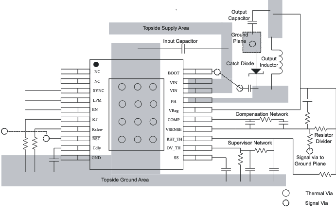
A proper layout is critical for the operation of a switched-mode power supply, even more at high switching frequencies. Therefore, the PCB layout of the TPS54262-Q1 device demands careful attention to ensure operation and to get the performance specified. A poor layout can lead to issues like poor regulation (line and load), stability and accuracy weaknesses, increased EMI radiation, and noise sensitivity. See Figure 29 for recommended layout example for TPS54262-Q1 device.
- It is critical to provide a low-inductance, low-impedance ground path and hence use wide and short traces for the main current paths.
- The input capacitor, catch diode, output capacitor, and inductor should be placed as close as possible to the IC pins and use thick traces (low impedance path) to connect them.
- Route the feedback trace so that there is minimum interaction with any noise sources associated with the switching components. Recommended practice is to place the inductor away from the feedback trace to prevent EMI noise.
- Place compensation network components away from switching components and route their connections away from noisy area.
- In a two-sided PCB, TI recommends having ground planes on both sides of the PCB to help reduce noise and ground-loop errors. Connect the ground connection for the input and output capacitors and IC ground to this ground plane.
- In a multilayer PCB, the ground plane separates the power plane (where high switching currents and components are placed) from the signal plane (where the feedback trace and components are) for improved performance.
- Also, arrange the components such that the switching-current loops curl in the same direction. Place the high-current components such that during conduction the current path is in the same direction. Doing so prevents magnetic field reversal caused by the traces between the two half cycles, helping to reduce radiated EMI.
- Add multiple thermal via's on the device thermal pad for better thermal performance.
10.2 Layout Example
 Figure 29. PCB Layout Example
10.3 Power Dissipation and Temperature Considerations
The power dissipation losses are applicable for continuous conduction mode operation (CCM). The total power dissipated by the device is the sum of the following power losses.
Conduction losses, PCON

Switching losses, PSW

Gate drive losses, PGate
Power supply losses, PIC
Therefore, the total power dissipated by the device is given by Equation 47.
where
- VIN = unregulated input voltage
- ILoad = output load current
- tr = FET switching rise time (tr= 40 ns (maximum))
- tf = FET switching fall time
- fsw = switching frequency
- Vdrive = FET gate drive voltage (Vdrive = 6 V (typical), Vdrive = 8 V (maximum))
- Qg = 1×10⁻⁹ C
- Iq-Normal = quiescent current in normal mode (Active Mode CCM)
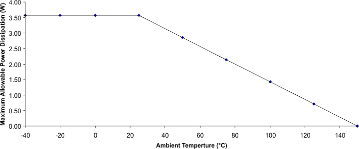
For device under operation at a given ambient temperature (TA), the junction temperature (TJ) can be calculated using Equation 48.
Therefore, the rise in junction temperature due to power dissipation is shown in Equation 49.
For a given maximum junction temperature (TJ-Max), the maximum ambient temperature (TA-Max) in which the device can operate is calculated using Equation 50.
where
- TJ = junction temperature in °C
- TA = ambient temperature in °C
- Rth = thermal resistance of package in W/°C
- TJ-Max = maximum junction temperature in °C
- TA-Max = maximum ambient temperature in °C
There are several other factors that also affect the overall efficiency and power losses. Examples of such factors are AC and DC losses in the inductor, voltage drop across the copper traces on PCB, power losses in the flyback catch diode and so forth. The previous discussion does not include such factors.
 Figure 30. Power Dissipation vs Ambient Temperature
NOTE
The output current rating for the regulator may must be derated for ambient temperatures above 85°C. The derated value will depend on calculated worst-case power dissipation and the thermal management implementation in the application.