SNVSBC0C September 2020 – December 2021 TPS542A50
PRODUCTION DATA
- 1 Features
- 2 Applications
- 3 Description
- 4 Revision History
- 5 Pin Configuration and Functions
- 6 Specifications
-
7 Detailed Description
- 7.1 Overview
- 7.2 Functional Block Diagram
- 7.3
Feature Description
- 7.3.1 Enable and Adjustable Undervoltage Lockout
- 7.3.2 Input and VREG Undervoltage Lockout Protection
- 7.3.3 Voltage Reference and Setting the Output Voltage
- 7.3.4 Remote Sense Function
- 7.3.5 Switching Frequency
- 7.3.6 Voltage Control Mode Internal Compensation
- 7.3.7 Soft Start and Prebiased Output Start-up
- 7.3.8 Power Good
- 7.3.9 Overvoltage and Undervoltage Protection
- 7.3.10 Overcurrent Protection
- 7.3.11 High-Side FET Throttling
- 7.3.12 Overtemperature Protection
- 7.4 Device Functional Modes
- 7.5 Programming
- 7.6 Pin-Strap Programming
- 7.7
Register Maps
- 7.7.1 ID Register (Offset = 0x0) [reset = 0x21]
- 7.7.2 STATUS Register (Offset = 0x1) [reset = 0x0]
- 7.7.3 VOUT_ADJ1 Register (Offset = 0x2) [reset = 0x0]
- 7.7.4 VOUT_ADJ2 Register (Offset = 0x3) [reset = 0x0]
- 7.7.5 CONFIG1 Register (Offset = 0x4) [reset = 0x0B]
- 7.7.6 CONFIG2 Register (Offset = 0x5) [reset = 0x2D]
-
8 Application and Implementation
- 8.1 Application Information
- 8.2
Typical Application
- 8.2.1
Full Analog Configuration
- 8.2.1.1 Design Requirements
- 8.2.1.2
Detailed Design Procedure
- 8.2.1.2.1 Custom Design With WEBENCH® Tools
- 8.2.1.2.2 Output Voltage Calculation
- 8.2.1.2.3 Switching Frequency Selection
- 8.2.1.2.4 Inductor Selection
- 8.2.1.2.5 Input Capacitor Selection
- 8.2.1.2.6 Bootstrap Capacitor Selection
- 8.2.1.2.7 R-C Snubber and VIN Pin High-Frequency Bypass
- 8.2.1.2.8 Output Capacitor Selection
- 8.2.1.2.9 Response to a Load Transient
- 8.2.1.2.10 Pin-Strap Setting
- 8.2.1.3 Application Curves
- 8.2.1.4 Typical Application Circuits
- 8.2.1
Full Analog Configuration
- 9 Power Supply Recommendations
- 10Layout
- 11Device and Documentation Support
- 12Mechanical, Packaging, and Orderable Information
Package Options
Mechanical Data (Package|Pins)
- RJM|33
Thermal pad, mechanical data (Package|Pins)
Orderable Information
3 Description
The TPS542A50 is a high-efficiency synchronous buck converter with differential remote sense and I2C. This device features fixed-frequency, voltage-control mode with pinstrap selectable internal compensation for reduced system cost and complexity. The PWM can be synchronized to an external clock through the SYNC pin. Other key features include PFM for high light load efficiency, low shutdown quiescent current draw, adjustable UVLO through the EN pin and monotonic start up into pre-biased conditions. This device also features an I2C interface for device configuration and output voltage adjustment. The TPS542A50 is a lead-free device. It is fully RoHS compliant without exemption.
| PART NUMBER | PACKAGE(1) | BODY SIZE (NOM) |
|---|---|---|
| TPS542A50 | VQFN (33) | 4.50 mm × 4.00 mm |
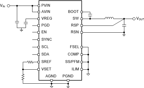
 Simplified Schematic
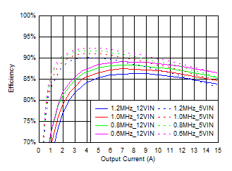
 Typical Efficiency at 1
VOUT