SLVS412F December 2001 – April 2019 TPS54310
PRODUCTION DATA.
- 1 Features
- 2 Applications
- 3 Description
- 4 Revision History
- 5 Device Comparison Table
- 6 Pin Configuration and Functions
- 7 Specifications
-
8 Detailed Description
- 8.1 Overview
- 8.2 Functional Block Diagram
- 8.3
Feature Description
- 8.3.1 Undervoltage Lockout (UVLO)
- 8.3.2 Slow Start and Enable (SS/ENA)
- 8.3.3 VBIAS Regulator (VBIAS)
- 8.3.4 Voltage Reference
- 8.3.5 Oscillator and PWM Ramp
- 8.3.6 Error Amplifier
- 8.3.7 PWM Control
- 8.3.8 Dead-Time Control and MOSFET Drivers
- 8.3.9 Overcurrent Protection
- 8.3.10 Thermal Shutdown
- 8.3.11 Powergood (PWRGD)
- 8.4 Device Functional Modes
- 9 Application and Implementation
- 10Power Supply Recommendations
- 11Layout
- 12Device and Documentation Support
- 13Mechanical, Packaging, and Orderable Information
Package Options
Mechanical Data (Package|Pins)
- PWP|20
Thermal pad, mechanical data (Package|Pins)
- PWP|20
Orderable Information
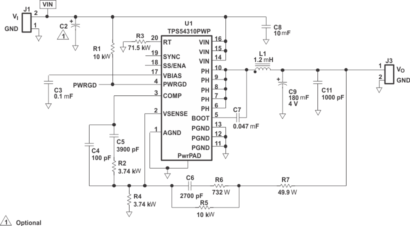
9.2 Typical Application
Figure 10 shows the schematic diagram for a typical TPS54310 application. The TPS54310 (U1) can provide up to 3 A of output current at a nominal output voltage of 3.3 V. For proper thermal performance, the power pad underneath the TPS54310 integrated circuit needs to be soldered well to the printed-circuit board.
 Figure 10. TPS54310 Schematic