SLVSAT1A June   2011  – July 2022 TPS54325-Q1

PRODUCTION DATA  

  1. Features
  2. Applications
  3. Description
  4. Revision History
  5. Pin Configuration and Functions
  6. Specifications
    1. 6.1 Absolute Maximum Ratings
    2. 6.2 ESD Ratings
    3. 6.3 Recommended Operating Conditions
    4. 6.4 Thermal Information
    5. 6.5 Electrical Characteristics
    6. 6.6 Typical Characteristics
  7. Detailed Description
    1. 7.1 Overview
    2. 7.2 Functional Block Diagram
    3. 7.3 Feature Description
      1. 7.3.1 Soft Start and Pre-Biased Soft Start
      2. 7.3.2 Power Good
      3. 7.3.3 Output Discharge Control
      4. 7.3.4 Current Protection
      5. 7.3.5 Overvoltage and Undervoltage Protection
      6. 7.3.6 UVLO Protection
      7. 7.3.7 Thermal Shutdown
    4. 7.4 Device Functional Modes
      1. 7.4.1 PWM Operation
      2. 7.4.2 PWM Frequency and Adaptive On-Time Control
  8. Application and Implementation
    1. 8.1 Application Information
    2. 8.2 Typical Application
      1. 8.2.1 Design Requirements
      2. 8.2.2 Detailed Design Procedure
        1. 8.2.2.1 Custom Design With WEBENCH® Tools
        2. 8.2.2.2 Output Inductor Selection
        3. 8.2.2.3 Output Capacitor Selection
        4. 8.2.2.4 Input Capacitor Selection
        5. 8.2.2.5 Bootstrap Capacitor Selection
        6. 8.2.2.6 VREG5 Capacitor Selection
        7. 8.2.2.7 Output Voltage Resistors Selection
      3. 8.2.3 Application Performance Plots
  9. Power Supply Recommendations
  10. 10Layout
    1. 10.1 Layout Guidelines
    2. 10.2 Layout Example
    3. 10.3 Thermal Information
  11. 11Device and Documentation Support
    1. 11.1 Device Support
      1. 11.1.1 Third-Party Products Disclaimer
      2. 11.1.2 Development Support
        1. 11.1.2.1 Custom Design With WEBENCH® Tools
    2. 11.2 Documentation Support
    3. 11.3 Receiving Notification of Documentation Updates
    4. 11.4 Support Resources
    5. 11.5 Trademarks
    6. 11.6 Electrostatic Discharge Caution
    7. 11.7 Glossary
  12. 12Mechanical, Packaging, and Orderable Information

Package Options

Mechanical Data (Package|Pins)
Thermal pad, mechanical data (Package|Pins)
Orderable Information

Description

The TPS54325-Q1 is an adaptive on-time D-CAP2 mode synchronous buck converter. The TPS54325-Q1 enables system designers to complete the suite of power bus regulators for various end equipments with a cost effective, low component count, low standby current solution. The main control loop for the TPS54325-Q1 uses the D-CAP2 mode control, which provides a very fast transient response with no external components. The TPS54325-Q1 also has a proprietary circuit that enables the device to adapt to both low equivalent series resistance (ESR) output capacitors, such as POSCAP or SP-CAP, and ultra-low ESR ceramic capacitors. The device operates from a 4.5-V to 18-V VCC input, and from a 2.0-V to 18-V VIN input power supply voltage. The output voltage can be programmed between 0.76 V and 5.5 V. The device also features an adjustable slow-start time and a power good function. The TPS54325-Q1 is available in the 14-pin HTSSOP package, and designed to operate from –40°C to 105°C.

Device Information
Part Number Package Body Size (NOM)
TPS54325-Q1 HTSSOP 5.00 mm × 4.40 mm
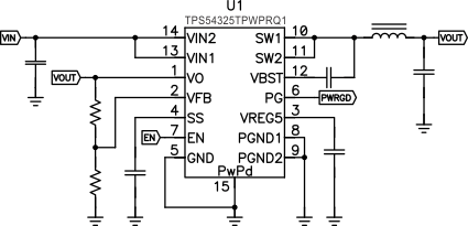
GUID-20220707-SS0I-5MBC-SRPL-TC2MN072QCJB-low.gifSimplified Schematic
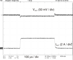
GUID-369BF245-0135-4023-BED2-A25D373AA756-low.gifLoad Transient Response