SLVS839H July 2008 – October 2023 TPS54331
PRODUCTION DATA
- 1
- 1 Features
- 2 Applications
- 3 Description
- 4 Revision History
- 5 Pin Configuration and Functions
- 6 Specifications
-
7 Detailed Description
- 7.1 Overview
- 7.2 Functional Block Diagram
- 7.3
Feature Description
- 7.3.1 Fixed-Frequency PWM Control
- 7.3.2 Voltage Reference (VREF)
- 7.3.3 Bootstrap Voltage (BOOT)
- 7.3.4 Enable and Adjustable Input Undervoltage Lockout (VIN UVLO)
- 7.3.5 Programmable Slow Start Using SS Pin
- 7.3.6 Error Amplifier
- 7.3.7 Slope Compensation
- 7.3.8 Current-Mode Compensation Design
- 7.3.9 Overcurrent Protection and Frequency Shift
- 7.3.10 Overvoltage Transient Protection
- 7.3.11 Thermal Shutdown
- 7.4 Device Functional Modes
-
8 Application and Implementation
- 8.1 Application Information
- 8.2
Typical Application
- 8.2.1 Design Requirements
- 8.2.2
Detailed Design Procedure
- 8.2.2.1 Custom Design with WEBENCH® Tools
- 8.2.2.2 Switching Frequency
- 8.2.2.3 Output Voltage Set-Point
- 8.2.2.4 Input Capacitors
- 8.2.2.5 Output Filter Components
- 8.2.2.6 Capacitor Selection
- 8.2.2.7 Compensation Components
- 8.2.2.8 Bootstrap Capacitor
- 8.2.2.9 Catch Diode
- 8.2.2.10 Output Voltage Limitations
- 8.2.2.11 Power Dissipation Estimate
- 8.2.3 Application Curves
- 8.3 Power Supply Recommendations
- 8.4 Layout
- 9 Device and Documentation Support
- 10Mechanical, Packaging, and Orderable Information
Package Options
Mechanical Data (Package|Pins)
Thermal pad, mechanical data (Package|Pins)
- DDA|8
Orderable Information
6.7 Typical Characteristics
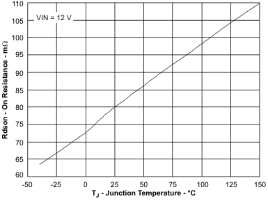
 Figure 6-1 ON
Resistance vs Junction Temperature
 Figure 6-3 Switching Frequency vs Junction Temperature
 Figure 6-5 Minimum Controllable On Time vs Junction Temperature
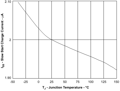
 Figure 6-7 SS
Charge Current vs Junction Temperature
 Figure 6-2 Shutdown Quiescent Current vs Input Voltage
 Figure 6-4 Voltage Reference vs Junction Temperature
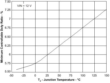
 Figure 6-6 Minimum Controllable Duty Ratio vs Junction Temperature
 Figure 6-8 Current-Limit Threshold vs Input Voltage