SLUSC26A May 2015 – February 2016 TPS54334
PRODUCTION DATA.
- 1 Features
- 2 Applications
- 3 Description
- 4 Revision History
- 5 Pin Configuration and Functions
- 6 Specifications
-
7 Detailed Description
- 7.1 Overview
- 7.2 Functional Block Diagram
- 7.3
Feature Description
- 7.3.1 Fixed Frequency PWM Control
- 7.3.2 Light Load Operation
- 7.3.3 Slope Compensation and Output Current
- 7.3.4 Bootstrap Voltage (BOOT) and Low Dropout Operation
- 7.3.5 Error Amplifier
- 7.3.6 Voltage Reference
- 7.3.7 Adjusting the Output Voltage
- 7.3.8 Enable and Undervoltage Lockout
- 7.3.9 Slow Start
- 7.3.10 Safe Start-up into Pre-Biased Outputs
- 7.3.11 Power Good (PGOOD)
- 7.4 Device Functional Modes
-
8 Application and Implementation
- 8.1 Application Information
- 8.2
Typical Applications
- 8.2.1
TPS54334 Application
- 8.2.1.1 Design Requirements
- 8.2.1.2 Detailed Design Procedure
- 8.2.1.3 Application Curves
- 8.2.1
TPS54334 Application
- 9 Power Supply Recommendations
- 10Layout
- 11Device and Documentation Support
- 12Mechanical, Packaging, and Orderable Information
Package Options
Mechanical Data (Package|Pins)
Thermal pad, mechanical data (Package|Pins)
- DDA|8
Orderable Information
1 Features
- Two 128mΩ/84mΩ MOSFETs for 3A Continuous Output Current
- Power Good
- Low 2 µA Shutdown Quiescent Current
- 0.8 V Internal Voltage Reference with ±1.5% Accuracy Over Temperature
- Fixed-Frequency Current Mode Control
- Pulse Skipping Boosts Efficiency at Light Loads
- Overcurrent Protection for Both MOSFETs with Hiccup Mode for Severe Fault Conditions
- Thermal and Overvoltage Transient Protection
- Available in Easy-to-Use 8-Pin SOIC PowerPAD™ and 10-Pin SON
- Monotonic Start-Up into Pre-biased Outputs
2 Applications
- Consumer Applications such as a Digital TV (DTV), Set Top Box (STB, DVD/Blu-ray Player), LCD Display, CPE (Cable Modem, WiFi Router), DLP Projectors, Smart Meters
- Battery Chargers
- Industrial and Car Audio Power Supplies
- 5V,12 and 24V Distributed Power Bus Supply
3 Description
The TPS54334 is a 28-V, 3-A, low quiescent supply current (IQ), synchronous monolithic buck converter with integrated MOSFETs.
The TPS54334 enables small designs by integrating the MOSFETs and implementing current mode control to reduce external component count.
Efficiency is maximized through the integrated 128mΩ/84mΩ MOSFETs, low quiescent supply current and pulse skipping at light loads. Using the enable pin, shutdown supply current is reduced to
2 µA by entering a shutdown mode.
The TPS54334 provides accurate regulation for a variety of loads with an accurate 1.5% voltage reference over temperature.
Cycle by cycle current limiting on the high-side fet protects the TPS54334 in overload situations and is enhanced by a low-side sourcing current limit which prevents current runaway. There is also a low-side sinking current limit which turns off the low-side MOSFET to prevent excessive reverse current. Hiccup protection will be triggered if the overcurrent condition has persisted for longer than the preset time. Thermal hiccup protection disables the part when die temperature exceeds thermal shutdown temperature and enables the part again after the built-in thermal hiccup time.
Device Information(1)
| PART NUMBER | PACKAGE | BODY SIZE (NOM) |
|---|---|---|
| TPS54334 | SO (8 Pin) | 4.89 mm × 3.90 mm |
| VSON (10 Pin) | 3.0 mm × 3.0 mm |
- For all available packages, see the orderable addendum at the end of the datasheet.
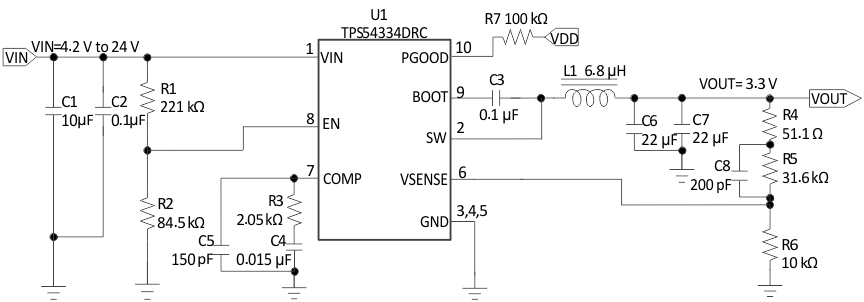
Simplified Schematic
