SLVS845G March   2009  – August 2014 TPS54362-Q1

PRODUCTION DATA.  

  1. Features
  2. Applications
  3. Description
  4. Revision History
  5. Pin Configuration and Functions
  6. Specifications
    1. 6.1 Absolute Maximum Ratings
    2. 6.2 Handling Ratings
    3. 6.3 Recommended Operating Conditions
    4. 6.4 Thermal Information
    5. 6.5 Electrical Characteristics
    6. 6.6 Timing Requirements
    7. 6.7 Switching Characteristics
    8. 6.8 Typical Characteristics
      1. 6.8.1 Efficiency Data of Power Supply
      2. 6.8.2 Output Voltage Dropout
      3. 6.8.3 Quiescent and Standby Current
      4. 6.8.4 Reference Voltages
  7. Detailed Description
    1. 7.1 Overview
    2. 7.2 Functional Block Diagram
    3. 7.3 Feature Description
      1. 7.3.1  Input Voltage
      2. 7.3.2  Function Mode
      3. 7.3.3  Output Voltage V(VReg)
      4. 7.3.4  Oscillator Frequency (RT)
      5. 7.3.5  Synchronization (SYNC)
      6. 7.3.6  Enable or Shutdown (EN)
      7. 7.3.7  Reset Delay (Cdly)
      8. 7.3.8  Reset Pin (RST)
      9. 7.3.9  Boost Capacitor (BOOT)
      10. 7.3.10 Soft Start (SS)
      11. 7.3.11 Short-Circuit Protection
      12. 7.3.12 Overcurrent Protection
      13. 7.3.13 Slew Rate Control (Rslew)
      14. 7.3.14 Thermal Shutdown
      15. 7.3.15 Regulation Voltage (VSENSE)
      16. 7.3.16 RESET Threshold (RST_TH)
      17. 7.3.17 Overvoltage Supervisor for V(VReg) (OV_TH)
      18. 7.3.18 Noise Filter on RST_TH and OV_TH Pins
      19. 7.3.19 Output Tolerances Based on Modes of Operation
      20. 7.3.20 Load Regulation and Line Regulation in Hysteretic Mode
      21. 7.3.21 Internal Undervoltage Lockout (UVLO)
      22. 7.3.22 Loop-Control Frequency Compensation
        1. 7.3.22.1 Type III Compensation
      23. 7.3.23 Bode Plot of Converter Gain
    4. 7.4 Device Functional Modes
      1. 7.4.1 Low-Power Mode (LPM)
      2. 7.4.2 Buck-Mode Low-Power-Mode Operation
      3. 7.4.3 External LPM Operation
  8. Application and Implementation
    1. 8.1 Application Information
    2. 8.2 Typical Application
      1. 8.2.1 Design Requirements
      2. 8.2.2 Detailed Design Procedure
        1. 8.2.2.1  Selecting the Switching Frequency
        2. 8.2.2.2  Output Inductor Selection (LO)
        3. 8.2.2.3  Output Capacitor (CO)
        4. 8.2.2.4  Flyback Schottky Diode
        5. 8.2.2.5  Input Capacitor, C(I)
        6. 8.2.2.6  Output Voltage and Feedback Resistor Selection
        7. 8.2.2.7  Overvoltage Resistor Selection
        8. 8.2.2.8  Reset-Threshold Resistor Selection
        9. 8.2.2.9  Low-Power Mode Threshold
        10. 8.2.2.10 Undervoltage Threshold for Low-Power Mode and Load-Transient Operation
        11. 8.2.2.11 Soft-Start Capacitor
        12. 8.2.2.12 Bootstrap Capacitor Selection
        13. 8.2.2.13 Guidelines for Compensation Components
        14. 8.2.2.14 Compensation
          1. 8.2.2.14.1 Calculate the Loop Compensation
          2. 8.2.2.14.2 Power Dissipation
      3. 8.2.3 Application Curves
  9. Power Supply Recommendations
  10. 10Layout
    1. 10.1 Layout Guidelines
      1. 10.1.1 Inductor
      2. 10.1.2 Input Filter Capacitors
      3. 10.1.3 Feedback
      4. 10.1.4 Traces and Ground Plane
    2. 10.2 Layout Example
  11. 11Device and Documentation Support
    1. 11.1 Trademarks
    2. 11.2 Electrostatic Discharge Caution
    3. 11.3 Glossary
  12. 12Mechanical, Packaging, and Orderable Information

Package Options

Mechanical Data (Package|Pins)
Thermal pad, mechanical data (Package|Pins)
Orderable Information

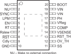
5 Pin Configuration and Functions

PWP 20-Pin Package
20-Pin HTSSOP With Thermal Pad
Top View
po_lvs845.gif

Pin Functions

PIN I/O DESCRIPTION
NAME NO.
BOOT 20 O External bootstrap capacitor to PH to drive the gate of the internal switching FET
Cdly 9 I/O External capacitor to ground to program power-on-reset delay.
COMP 15 I/O Error-amplifier output to connect external compensation components
EN 5 I Enable pin, internally pulled up. This pin requires an external pullup or pulldown to enable or disable the device.
GND 10 O Ground pin
LPM 4 I Low-power mode control using digital input signal. An internal pulldown resistor of 62 kΩ (typical) connects to ground.
NU 1 Connect to ground
2
OV_TH 12 I Sense input for overvoltage detection on regulated output. This pin monitors the V(Vreg)output voltage as divided by the external resistor network connecting between the VReg pin and ground. The resistor network programs the threshold voltage.
PH 17 O Source of the internal switching FET
Rslew 7 O External resistor to ground to control the slew rate of the internal switching FET
RST 8 O Active-low, open-drain reset output connected to external bias voltage through a resistor, asserted high after the device starts regulating
RST_TH 13 I Sense input for undervoltage and reset voltage detection on regulated output to initiate a reset-output signal. This pin monitors the V(Vreg) output voltage as divided by the external resistor network connecting between the VReg pin and ground. The resistor network programs the threshold voltage.
RT 6 O External resistor to ground to program the internal oscillator frequency
SS 11 I/O External capacitor to ground to program soft-start time
SYNC 3 I External synchronization clock input to override the internal oscillator clock. An internal pulldown resistor of 62 kΩ (typical) connects to ground.
VIN 18 I Unregulated input voltage. Connect pin 18 and pin 19 together externally.
19
VReg 16 I Internal low-side FET to load output during start-up or limit overshoot
VSENSE 14 I Inverting node of error amplifier for voltage-mode control
Thermal pad The thermal pad connects electrically to exposed ground pad on PCB for proper thermal performance.