SLUSCD4B March 2017 – May 2018 TPS543C20
PRODUCTION DATA.
- 1 Features
- 2 Applications
- 3 Description
- 4 Revision History
- 5 Device Comparison Table
- 6 Pin Configuration and Functions
- 7 Specifications
-
8 Detailed Description
- 8.1 Overview
- 8.2 Functional Block Diagram
- 8.3 Feature Description
- 8.4
Device Functional Modes
- 8.4.1 Soft-Start Operation
- 8.4.2 Input and VDD Undervoltage Lockout (UVLO) Protection
- 8.4.3 Power Good and Enable
- 8.4.4 Voltage Reference
- 8.4.5 Prebiased Output Start-up
- 8.4.6 Internal Ramp Generator
- 8.4.7 Switching Frequency
- 8.4.8 Clock Sync Point Selection
- 8.4.9 Synchronization and Stackable Configuration
- 8.4.10 Dual-Phase Stackable Configurations
- 8.4.11 Operation Mode
- 8.4.12 API/BODY Brake
- 8.4.13 Sense and Overcurrent Protection
- 8.4.14 Output Overvoltage and Undervoltage Protection
- 8.4.15 Overtemperature Protection
- 8.4.16 RSP/RSN Remote Sense Function
- 8.4.17 Current Sharing
- 8.4.18 Loss of Synchronization
-
9 Application and Implementation
- 9.1 Application Information
- 9.2
Typical Application: TPS543C20 Stand-alone Device
- 9.2.1 Design Requirements
- 9.2.2 Detailed Design Procedure
- 9.2.3 Application Curves
- 9.3 System Example
- 10Power Supply Recommendations
- 11Layout
- 12Device and Documentation Support
- 13Mechanical, Packaging, and Orderable Information
Package Options
Mechanical Data (Package|Pins)
- RVF|40
Thermal pad, mechanical data (Package|Pins)
- RVF|40
Orderable Information
8.4.16 RSP/RSN Remote Sense Function
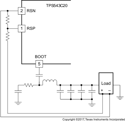
RSP and RSN pins are used for remote sensing purpose. In the case where feedback resistors are required for output voltage programming, the RSP pin should be connected to the mid-point of the resistor divider and the RSN pin should always be connected to the load return.
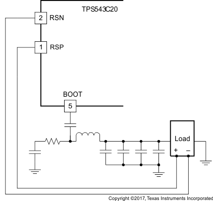
In the case where feedback resistors are not required as when the VSEL programs the output voltage set point, the RSP pin should be connected to the positive sensing point of the load and the RSN pin should always be connected to the load return. RSP and RSN pins are extremely high-impedance input terminals of the true differential remote sense amplifier. The feedback resistor divider should use resistor values much less than 100 kΩ. A simple rule of thumb is to use a 10-kΩ lower divider resistor and then size the upper resistor to achieve the desired ratio.
 Figure 22. Remote Sensing With Feedback Resistors
 Figure 23. Remote Sensing Without Feedback Resistors