SLUSDE0 December 2018 TPS543C20A
PRODUCTION DATA.
- 1 Features
- 2 Applications
- 3 Description
- 4 Revision History
- 5 Device Comparison Table
- 6 Pin Configuration and Functions
- 7 Specifications
-
8 Detailed Description
- 8.1 Overview
- 8.2 Functional Block Diagram
- 8.3 Feature Description
- 8.4
Device Functional Modes
- 8.4.1 Soft-Start Operation
- 8.4.2 Input and VDD Undervoltage Lockout (UVLO) Protection
- 8.4.3 Power Good and Enable
- 8.4.4 Voltage Reference
- 8.4.5 Prebiased Output Start-up
- 8.4.6 Internal Ramp Generator
- 8.4.7 Switching Frequency
- 8.4.8 Clock Sync Point Selection
- 8.4.9 Synchronization and Stackable Configuration
- 8.4.10 Dual-Phase Stackable Configurations
- 8.4.11 Operation Mode
- 8.4.12 API/Body Brake
- 8.4.13 Sense and Overcurrent Protection
- 8.4.14 Output Overvoltage and Undervoltage Protection
- 8.4.15 Overtemperature Protection
- 8.4.16 RSP/RSN Remote Sense Function
- 8.4.17 Current Sharing
- 8.4.18 Loss of Synchronization
-
9 Application and Implementation
- 9.1 Application Information
- 9.2
Typical Application: TPS543C20A Stand-alone Device
- 9.2.1 Design Requirements
- 9.2.2 Detailed Design Procedure
- 9.2.3 Application Curves
- 9.3 System Example
- 10Power Supply Recommendations
- 11Layout
- 12Device and Documentation Support
- 13Mechanical, Packaging, and Orderable Information
Package Options
Mechanical Data (Package|Pins)
- RVF|40
Thermal pad, mechanical data (Package|Pins)
- RVF|40
Orderable Information
9.2.3 Application Curves
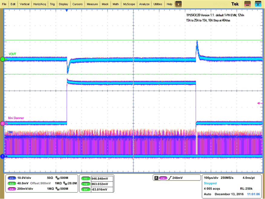 Figure 27. Transient Response of 0.9-V Output at 12-VIN,
Transient is 15 A to 25 A to 15 A,
the Step is 10 A at 40 A/μs
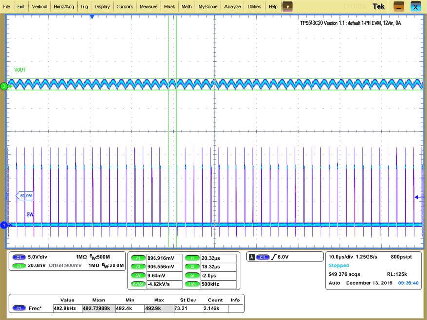 Figure 29. Output Ripple and SW Node of 0.9-V Output at 12-VIN, 0-A Output
 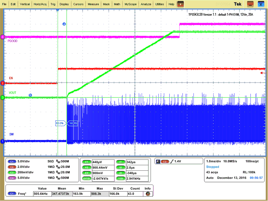 Figure 31. 0.5-V Prebias start up from Control, 0.9-V Output at 12-VIN, 20-A Output
 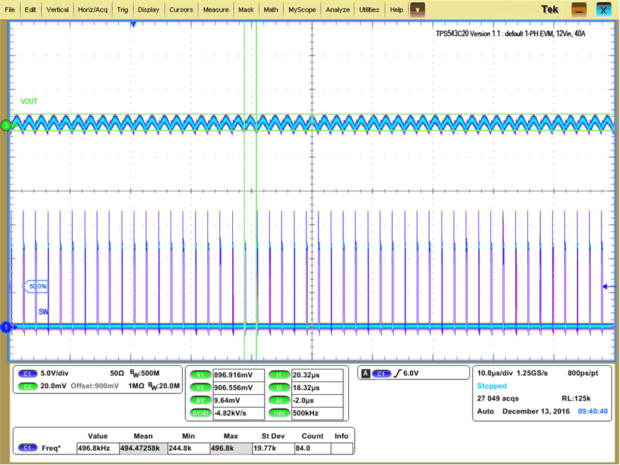 Figure 28. Output Ripple and SW Node of 0.9-V Output at 12-VIN, -A Output
 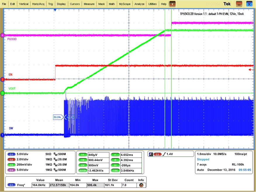 Figure 30. Start up from Control, 0.9-V Output at 12-VIN, 10-mA Output
 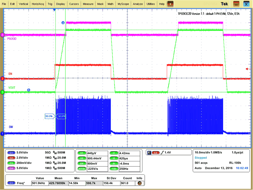 Figure 32. Output Voltage Start-up and Shutdown, 0.9-V Output at 12-VIN, 0.5-A Output