SLUSB69B May 2014 – July 2016 TPS544B20 , TPS544C20
PRODUCTION DATA.
- 1 Features
- 2 Applications
- 3 Description
- 4 Revision History
- 5 Device Comparison Table
- 6 Pin Configuration and Functions
- 7 Specifications
-
8 Detailed Description
- 8.1 Overview
- 8.2 Functional Block Diagram
- 8.3
Feature Description
- 8.3.1 Turn-On and Turn-Off Delay and Sequencing
- 8.3.2 Pre-Biased Output Start-Up
- 8.3.3 Voltage Reference
- 8.3.4 Differential Remote Sense and Output Voltage Setting
- 8.3.5 PMBus Output Voltage Adjustment
- 8.3.6 Switching Frequency
- 8.3.7 Soft-Start
- 8.3.8 Linear Regulators BP3 and BP6
- 8.3.9 External Bypass (BPEXT)
- 8.3.10 Current Monitoring and Low-Side MOSFET Overcurrent Protection
- 8.3.11 High-Side MOSFET Short-Circuit Protection
- 8.3.12 Over-Temperature Protection
- 8.3.13 Input Undervoltage Lockout (UVLO)
- 8.3.14 Output Overvoltage and Undervoltage Protection
- 8.3.15 Fault Protection Responses
- 8.3.16 PMBus General Description
- 8.3.17 PMBus Address
- 8.3.18 PMBus Connections
- 8.3.19 Auto ARA (Alert Response Address) Response
- 8.4 Device Functional Modes
- 8.5 Programming
- 8.6
Register Maps
- 8.6.1 OPERATION (01h)
- 8.6.2 ON_OFF_CONFIG (02h)
- 8.6.3 CLEAR_FAULTS (03h)
- 8.6.4 WRITE_PROTECT (10h)
- 8.6.5 STORE_USER_ALL (15h)
- 8.6.6 RESTORE_USER_ALL (16h)
- 8.6.7 CAPABILITY (19h)
- 8.6.8 VOUT_MODE (20h)
- 8.6.9 VIN_ON (35h)
- 8.6.10 VIN_OFF (36h)
- 8.6.11 IOUT_CAL_OFFSET (39h)
- 8.6.12 IOUT_OC_FAULT_LIMIT (46h)
- 8.6.13 IOUT_OC_FAULT_RESPONSE (47h)
- 8.6.14 IOUT_OC_WARN_LIMIT (4Ah)
- 8.6.15 OT_FAULT_LIMIT (4Fh)
- 8.6.16 OT_WARN_LIMIT (51h)
- 8.6.17 TON_RISE (61h)
- 8.6.18 STATUS_BYTE (78h)
- 8.6.19 STATUS_WORD (79h)
- 8.6.20 STATUS_VOUT (7Ah)
- 8.6.21 STATUS_IOUT (7Bh)
- 8.6.22 STATUS_TEMPERATURE (7Dh)
- 8.6.23 STATUS_CML (7Eh)
- 8.6.24 STATUS_MFR_SPECIFIC (80h)
- 8.6.25 READ_VOUT (8Bh)
- 8.6.26 READ_IOUT (8Ch)
- 8.6.27 READ_TEMPERATURE_2 (8Eh)
- 8.6.28 PMBUS_REVISION (98h)
- 8.6.29 MFR_SPECIFIC_00 (D0h)
- 8.6.30 VREF_TRIM (MFR_SPECIFIC_04) (D4h)
- 8.6.31 STEP_VREF_MARGIN_HIGH (MFR_SPECIFIC_05) (D5h)
- 8.6.32 STEP_VREF_MARGIN_LOW (MFR_SPECIFIC_06) (D6h)
- 8.6.33 PCT_VOUT_FAULT_PG_LIMIT (MFR_SPECIFIC_07) (D7h)
- 8.6.34 SEQUENCE_TON_TOFF_DELAY (MFR_SPECIFIC_08) (D8h)
- 8.6.35 OPTIONS (MFR_SPECIFIC_21) (E5h)
- 8.6.36 MASK_SMBALERT (MFR_SPECIFIC_23) (E7h)
- 8.6.37 DEVICE_CODE (MFR_SPECIFIC_44) (FCh)
-
9 Applications and Implementation
- 9.1 Application Information
- 9.2
Typical Application
- 9.2.1 Design Requirements
- 9.2.2
Detailed Design Procedure
- 9.2.2.1 Switching Frequency Selection
- 9.2.2.2 Inductor Selection
- 9.2.2.3 Output Capacitor Selection
- 9.2.2.4 D-CAP Mode and D-CAP2 Mode Stability
- 9.2.2.5 Input Capacitor Selection
- 9.2.2.6 Bootstrap Capacitor and Resistor Selection
- 9.2.2.7 BP6, BP3 and BPEXT
- 9.2.2.8 R-C Snubber and VIN Pin High-Frequency Bypass
- 9.2.2.9 Temperature Sensor
- 9.2.2.10 Key PMBus Parameter Selection
- 9.2.2.11 Output Voltage Setting and Frequency Compensation Selection
- 9.2.3 Application Curves
- 10Power Supply Recommendations
- 11Layout
- 12Device and Documentation Support
- 13Mechanical, Packaging, and Orderable Information
Package Options
Mechanical Data (Package|Pins)
- RVF|40
Thermal pad, mechanical data (Package|Pins)
- RVF|40
Orderable Information
12 Device and Documentation Support
12.1 Device Support
12.1.1 Development Support
12.1.1.1 Texas Instruments Fusion Digital Power™ Designer
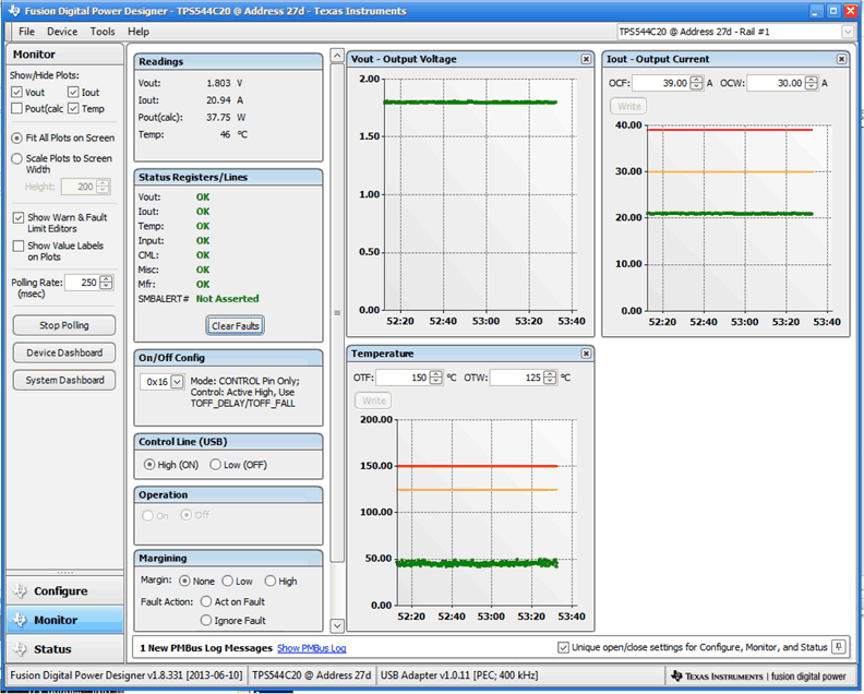
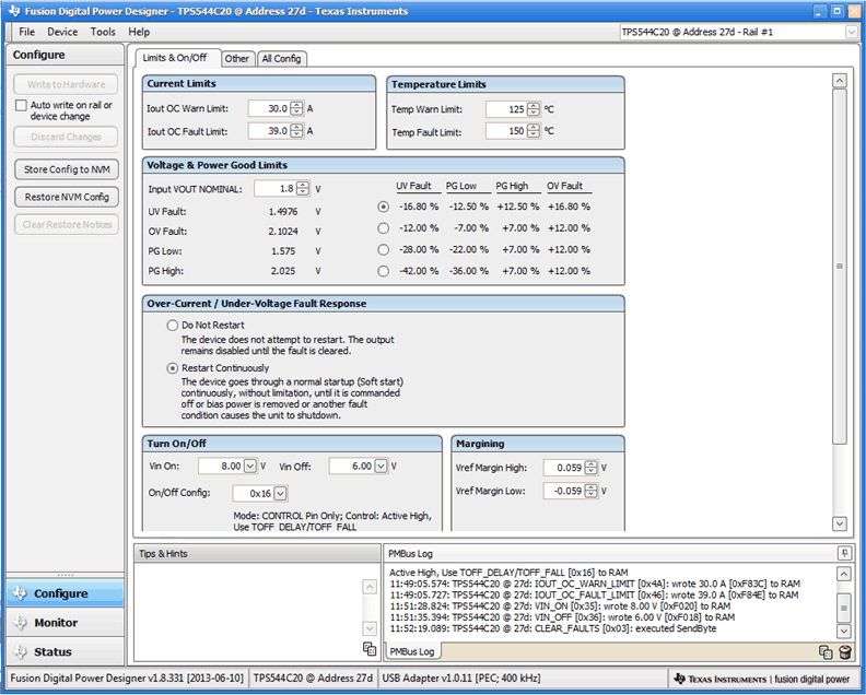
The TPS544B20 and TPS544C20 devices are fully supported by Texas Instruments Digital Power Designer. Fusion Digital Power Designer is a graphical user interface (GUI) used to configure and monitor the TPS544B20 and TPS544C20 devices according to the PMBus interface protocol via a Texas Instruments USB-to-GPIO adapter.
Click this link to download the Texas Instruments Fusion Digital Power Designer software package.
 Figure 48. Device Monitoring with Fusion Digital Power Designer
 Figure 49. Device Configuration with Fusion Digital Power Designer
12.2 Related Links
The table below lists quick access links. Categories include technical documents, support and community resources, tools and software, and quick access to sample or buy.
Table 13. Related Links
| PARTS | PRODUCT FOLDER | SAMPLE & BUY | TECHNICAL DOCUMENTS | TOOLS & SOFTWARE | SUPPORT & COMMUNITY |
|---|---|---|---|---|---|
| TPS544B20 | Click here | Click here | Click here | Click here | Click here |
| TPS544C20 | Click here | Click here | Click here | Click here | Click here |
12.3 Trademarks
E2E is a trademark of Texas Instruments.
NexFET, D-CAP, D-CAP2, Fusion Digital Power are trademarks of TI.
All other trademarks are the property of their respective owners.
12.4 Receiving Notification of Documentation Updates
To receive notification of documentation updates, navigate to the device product folder on ti.com. In the upper right corner, click on Alert me to register and receive a weekly digest of any product information that has changed. For change details, review the revision history included in any revised document.
12.5 Community Resources
The following links connect to TI community resources. Linked contents are provided "AS IS" by the respective contributors. They do not constitute TI specifications and do not necessarily reflect TI's views; see TI's Terms of Use.
-
TI E2E™ Online Community TI's Engineer-to-Engineer (E2E) Community. Created to foster collaboration among engineers. At e2e.ti.com, you can ask questions, share knowledge, explore ideas and help solve problems with fellow engineers.
-
Design Support TI's Design Support Quickly find helpful E2E forums along with design support tools and contact information for technical support.
12.6 Electrostatic Discharge Caution

These devices have limited built-in ESD protection. The leads should be shorted together or the device placed in conductive foam during storage or handling to prevent electrostatic damage to the MOS gates.
12.7 Glossary
SLYZ022 — TI Glossary.
This glossary lists and explains terms, acronyms, and definitions.