SLVS757E March 2007 – July 2022 TPS5450
PRODUCTION DATA
- 1 Features
- 2 Applications
- 3 Description
- 4 Revision History
- 5 Pin Configuration and Functions
- 6 Specifications
-
7 Detailed Description
- 7.1 Overview
- 7.2 Functional Block Diagram
- 7.3
Feature Description
- 7.3.1 Oscillator Frequency
- 7.3.2 Voltage Reference
- 7.3.3 Enable (ENA) and Internal Slow-Start
- 7.3.4 Undervoltage Lockout (UVLO)
- 7.3.5 Boost Capacitor (BOOT)
- 7.3.6 Output Feedback (VSENSE) and Internal Compensation
- 7.3.7 Voltage Feed-Forward
- 7.3.8 Pulse-Width-Modulation (PWM) Control
- 7.3.9 Overcurrent Limiting
- 7.3.10 Overvoltage Protection
- 7.3.11 Thermal Shutdown
- 7.4 Device Functional Modes
-
8 Application and Implementation
- 8.1 Application Information
- 8.2
Typical Application
- 8.2.1 Design Requirements
- 8.2.2 Detailed Design Procedure
- 8.2.3 Application Curves
- 9 Power Supply Recommendations
- 10Layout
- 11Device and Documentation Support
- 12Mechanical, Packaging, and Orderable Information
Package Options
Refer to the PDF data sheet for device specific package drawings
Mechanical Data (Package|Pins)
- DDA|8
Thermal pad, mechanical data (Package|Pins)
- DDA|8
Orderable Information
8.2.2.6 Capacitor Selection
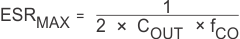
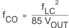
The important design factors for the output capacitor are DC voltage rating, ripple current rating, and equivalent series resistance (ESR). The DC voltage and ripple current ratings cannot be exceeded. The ESR is important because along with the inductor ripple current it determines the amount of output ripple voltage. The actual value of the output capacitor is not critical, but some practical limits do exist. Consider the relationship between the desired closed-loop crossover frequency of the design and LC corner frequency of the output filter. Due to the design of the internal compensation, it is desirable to keep the closed-loop crossover frequency in the range 3 kHz to 30 kHz as this frequency range has adequate phase boost to allow for stable operation. For this design example, it is assumed that the intended closed-loop crossover frequency will be between 2590 Hz and 24 kHz and also below the ESR zero of the output capacitor. Under these conditions the closed-loop crossover frequency is related to the LC corner frequency by:
And the desired output capacitor value for the output filter to:
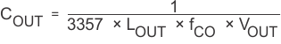
For a desired crossover of 12 kHz and a 15-μH inductor, the calculated value for the output capacitor is 330 μF. The capacitor type should be chosen so that the ESR zero is above the loop crossover. The maximum ESR should be: