SLVS757E March 2007 – July 2022 TPS5450
PRODUCTION DATA
- 1 Features
- 2 Applications
- 3 Description
- 4 Revision History
- 5 Pin Configuration and Functions
- 6 Specifications
-
7 Detailed Description
- 7.1 Overview
- 7.2 Functional Block Diagram
- 7.3
Feature Description
- 7.3.1 Oscillator Frequency
- 7.3.2 Voltage Reference
- 7.3.3 Enable (ENA) and Internal Slow-Start
- 7.3.4 Undervoltage Lockout (UVLO)
- 7.3.5 Boost Capacitor (BOOT)
- 7.3.6 Output Feedback (VSENSE) and Internal Compensation
- 7.3.7 Voltage Feed-Forward
- 7.3.8 Pulse-Width-Modulation (PWM) Control
- 7.3.9 Overcurrent Limiting
- 7.3.10 Overvoltage Protection
- 7.3.11 Thermal Shutdown
- 7.4 Device Functional Modes
-
8 Application and Implementation
- 8.1 Application Information
- 8.2
Typical Application
- 8.2.1 Design Requirements
- 8.2.2 Detailed Design Procedure
- 8.2.3 Application Curves
- 9 Power Supply Recommendations
- 10Layout
- 11Device and Documentation Support
- 12Mechanical, Packaging, and Orderable Information
Package Options
Refer to the PDF data sheet for device specific package drawings
Mechanical Data (Package|Pins)
- DDA|8
Thermal pad, mechanical data (Package|Pins)
- DDA|8
Orderable Information
The maximum ESR of the output capacitor also determines the amount of output ripple as specified in the initial design parameters. The output ripple voltage is the inductor ripple current times the ESR of the output filter. Check that the maximum specified ESR as listed in the capacitor data sheet results in an acceptable output ripple voltage:
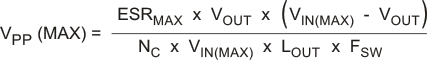
where
- ΔVPP is the desired peak-to-peak output ripple.
- NC is the number of parallel output capacitors.
- FSW is the switching frequency.
For this design example, a single 330-μF output capacitor is chosen for C3. The calculated RMS ripple current is 143 mA and the maximum ESR required is 40 mΩ. A capacitor that meets these requirements is a Sanyo Poscap 10TPB330M, rated at 10 V with a maximum ESR of 35 mΩ and a ripple current rating of 3 A. An additional small 0.1-μF ceramic bypass capacitor, C6 is also used in this design.
The minimum ESR of the output capacitor should also be considered. For good phase margin, the ESR zero when the ESR is at a minimum should not be too far above the internal compensation poles at 24 kHz and 54 kHz.
The selected output capacitor must also be rated for a voltage greater than the desired output voltage plus one half the ripple voltage. Any derating amount must also be included. The maximum RMS ripple current in the output capacitor is given by Equation 12:
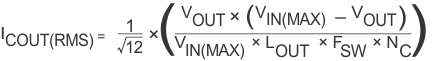
where
- NC is the number of output capacitors in parallel.
- FSW is the switching frequency.
Other capacitor types can be used with the TPS5450, depending on the needs of the application.