SLVSB82B May 2012 – April 2021 TPS54525
PRODUCTION DATA
- 1 Features
- 2 Applications
- 3 Description
- 4 Revision History
- 5 Pin Configuration and Functions
- 6 Specifications
- 7 Detailed Description
- 8 Application and Implementation
- 9 Power Supply Recommendations
- 10Layout
- 11Device and Documentation Support
Package Options
Mechanical Data (Package|Pins)
- PWP|14
Thermal pad, mechanical data (Package|Pins)
- PWP|14
Orderable Information
6.6 Typical Characteristics
VIN = 12 V, TA = 25 °C (unless otherwise noted)
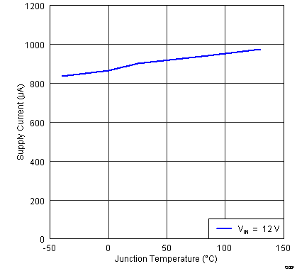 Figure 6-1 VIN Current vs
Junction Temperature
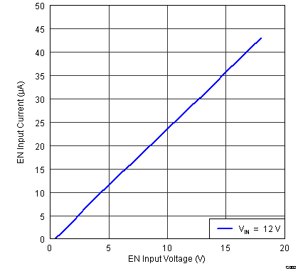 Figure 6-3 EN Current vs EN
Voltage
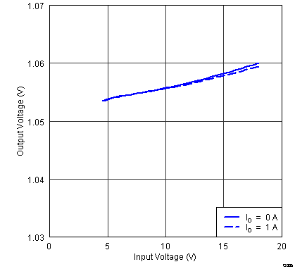 Figure 6-5 1.05-V Output Voltage vs
Input Voltage
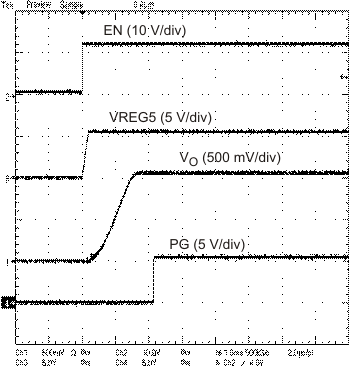 Figure 6-7 Start-Up Waveform
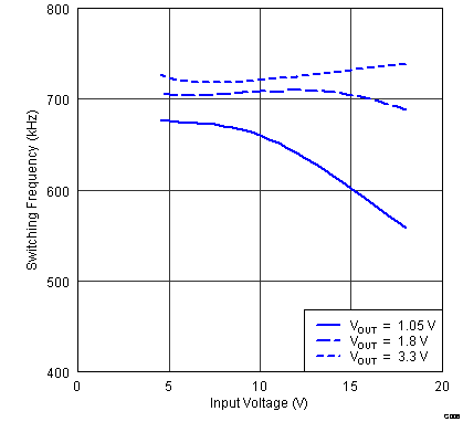 Figure 6-9 Switching Frequency vs
Input Voltage (IO = 1 A)
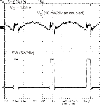 Figure 6-11 Voltage Ripple at Outptut
(IO = 5.5 A)
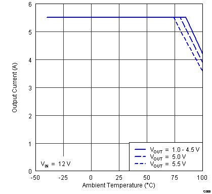 Figure 6-13 Output Current vs Ambient
Temperature
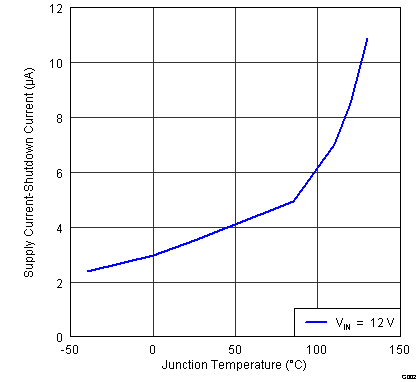 Figure 6-2 VIN Shutdown
Current vs Junction Temperature
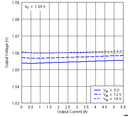 Figure 6-4 1.05-V Output Voltage vs
Output Current
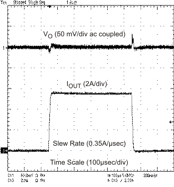 Figure 6-6 1.05-V, 50-mA to 5.5-A
Load Transient Response
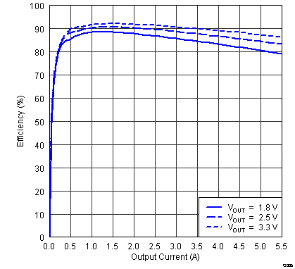 Figure 6-8 Efficiency vs Output
Current
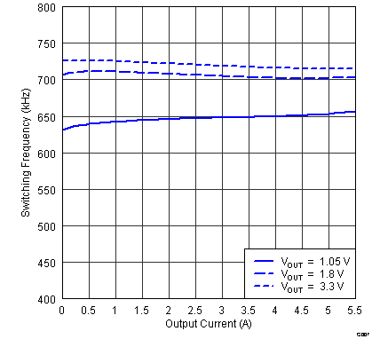 Figure 6-10 Switching Frequency vs
Output Current
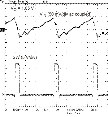 Figure 6-12 Voltage Ripple at Input
(IO = 5.5 A)