SLVSB84D May 2012 – April 2021 TPS54526
PRODUCTION DATA
- 1 Features
- 2 Applications
- 3 Description
- 4 Revision History
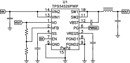
- 5 Pin Configuration and Functions
- 6 Specifications
- 7 Detailed Description
- 8 Application and Implementation
- 9 Power Supply Recommendations
- 10Layout
- 11Device and Documentation Support
- 12Mechanical, Packaging, and Orderable Information
Package Options
Mechanical Data (Package|Pins)
Thermal pad, mechanical data (Package|Pins)
- RSA|16
Orderable Information
3 Description
The TPS54526 is an adaptive on-time D-CAP2™ mode synchronous buck converter. The TPS54526 enables system designers to complete the suite of various end equipment’s power bus regulators with a cost effective, low component count, low standby current solution. The main control loop for the TPS54526 uses the D-CAP2™ mode control which provides a very fast transient response with no external compensation components. The adaptive on-time control supports seamless transition between PWM mode at higher load conditions and Eco-mode™ operation at light loads. Eco-mode™ allows the TPS54526 to maintain high efficiency during lighter load conditions. The TPS54526 also has a proprietary circuit that enables the device to adopt to both low equivalent series resistance (ESR) output capacitors, such as POSCAP, SP-CAP, and ultra-low ESR ceramic capacitors. The device operates from 4.5-V to 18-V VIN input. The output voltage can be programmed between 0.76V and 5.5V. The device also features an adjustable soft start time and a power good function. The TPS54526 is available in the 14-pin HTSSOP package and the 16 pin QFN package, designed to operate from –40°C to 85°C.
| PART NUMBER | PACKAGE | BODY SIZE (NOM) |
|---|---|---|
| TPS54526 | HTSSOP (14) | 5.00mm x 4.40mm |
| VQFN (16) | 4.00mm x 4.00mm |