SLVSB84D May   2012  – April 2021 TPS54526

PRODUCTION DATA  

  1. Features
  2. Applications
  3. Description
  4. Revision History
  5. Pin Configuration and Functions
  6. Specifications
    1. 6.1 Absolute Maximum Ratings
    2. 6.2 Handling Ratings
    3. 6.3 Recommended Operating Conditions
    4. 6.4 Thermal Information
    5. 6.5 Electrical Characteristics
    6. 6.6 Timing Requirements
    7. 6.7 Typical Characteristics
  7. Detailed Description
    1. 7.1 Overview
    2. 7.2 Functional Block Diagram
    3. 7.3 Feature Description
      1. 7.3.1  PWM Operation
      2. 7.3.2  PWM Frequency and Adaptive On-Time Control
      3. 7.3.3  Soft Start and Pre-Biased Soft Start
      4. 7.3.4  Power Good
      5. 7.3.5  VREG5
      6. 7.3.6  Output Discharge Control
      7. 7.3.7  Current Protection
      8. 7.3.8  Over/Under Voltage Protection
      9. 7.3.9  UVLO Protection
      10. 7.3.10 Thermal Shutdown
    4. 7.4 Device Functional Modes
      1. 7.4.1 Auto-Skip Eco-Mode™ Control
  8. Application and Implementation
    1. 8.1 Application Information
    2. 8.2 Typical Application
      1. 8.2.1 Design Requirements
      2. 8.2.2 Detailed Design Procedure
        1. 8.2.2.1 Step By Step Design Procedure
        2. 8.2.2.2 Output Voltage Resistors Selection
        3. 8.2.2.3 Output Filter Selection
        4. 8.2.2.4 Input Capacitor Selection
        5. 8.2.2.5 Bootstrap Capacitor Selection
        6. 8.2.2.6 VREG5 Capacitor Selection
      3. 8.2.3 Application Curve
  9. Power Supply Recommendations
  10. 10Layout
    1. 10.1 Layout Guidelines
    2. 10.2 Layout Example
  11. 11Device and Documentation Support
    1. 11.1 Receiving Notification of Documentation Updates
    2. 11.2 Support Resources
    3. 11.3 Trademarks
    4. 11.4 Electrostatic Discharge Caution
    5. 11.5 Glossary
  12. 12Mechanical, Packaging, and Orderable Information
    1. 12.1 Thermal Information

Package Options

Mechanical Data (Package|Pins)
Thermal pad, mechanical data (Package|Pins)
Orderable Information

Application Curve

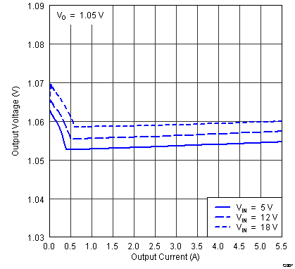
GUID-C9DCB63B-EADC-4A3D-B95A-137E27FD3926-low.pngFigure 8-2 1.05V Output Voltage vs Output Current
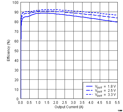
GUID-3A4D23DD-F063-4F31-8B04-38545F8473E5-low.pngFigure 8-4 Efficiency vs Output Current
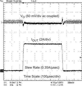
GUID-30B4B778-58DC-4C7C-8E61-7DD8562C9171-low.gif
1.05 V50 mA to 5.5 A
Figure 8-6 Load Transient Response
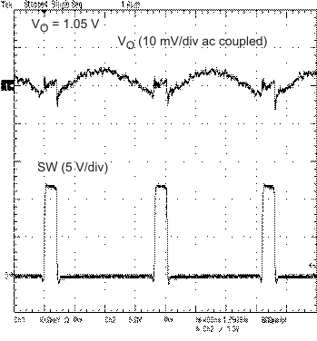
GUID-6B7BE3A5-28AD-4F9D-9A16-170FED1D14B4-low.gif
IO= 5.5A
Figure 8-8 Voltage Ripple at Output
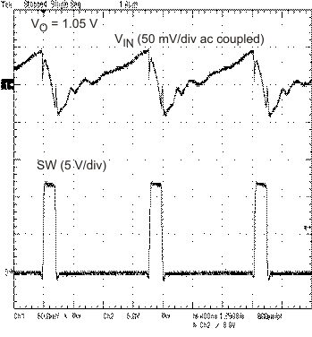
GUID-ECD6A4AE-246D-4A56-AB2B-926EA08F2A07-low.gif
IO= 5.5A
Figure 8-10 Voltage Ripple at Input
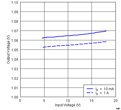
GUID-544025D6-CC00-4A67-B621-3810BE03AE0A-low.pngFigure 8-3 1.05V Output Voltage vs Input Voltage
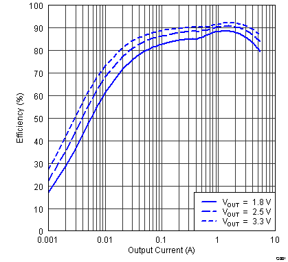
GUID-8CF0466C-5D2A-4E21-A144-4865F6AA394C-low.pngFigure 8-5 Light Load Efficiency vs Output Current
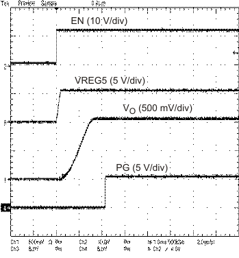
GUID-4C196070-C0B3-4FB4-8C7B-53C3D9111D90-low.gifFigure 8-7 Startup Waveform
GUID-6F1D9A94-0ADD-4F62-BAF4-38F6DD600E90-low.gif
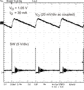
IO = 30 mA
Figure 8-9 Eco-mode Voltage Ripple at Output