SLVSF00 January 2019 TPS54560B
PRODUCTION DATA.
- 1 Features
- 2 Applications
- 3 Description
- 4 Revision History
- 5 Pin Configuration and Functions
- 6 Specifications
-
7 Detailed Description
- 7.1 Overview
- 7.2 Functional Block Diagram
- 7.3
Feature Description
- 7.3.1 Fixed Frequency PWM Control
- 7.3.2 Slope Compensation Output Current
- 7.3.3 Pulse Skip Eco-mode
- 7.3.4 Low Dropout Operation and Bootstrap Voltage (BOOT)
- 7.3.5 Error Amplifier
- 7.3.6 Adjusting the Output Voltage
- 7.3.7 Enable and Adjusting Undervoltage Lockout
- 7.3.8 Internal Soft Start
- 7.3.9 Constant Switching Frequency and Timing Resistor (RT/CLK) pin)
- 7.3.10 Accurate Current-Limit Operation and Maximum Switching Frequency
- 7.3.11 Synchronization to RT/CLK pin
- 7.3.12 Overvoltage Protection
- 7.3.13 Thermal Shutdown
- 7.3.14 Small Signal Model for Loop Response
- 7.3.15 Simple Small Signal Model for Peak-Current-Mode Control
- 7.3.16 Small Signal Model for Frequency Compensation
- 7.4 Device Functional Modes
-
8 Application and Implementation
- 8.1 Application Information
- 8.2
Typical Application
- 8.2.1 Design Requirements
- 8.2.2
Detailed Design Procedure
- 8.2.2.1 Custom Design with WEBENCH® Tools
- 8.2.2.2 Selecting the Switching Frequency
- 8.2.2.3 Output Inductor Selection (LO)
- 8.2.2.4 Output Capacitor
- 8.2.2.5 Catch Diode
- 8.2.2.6 Input Capacitor
- 8.2.2.7 Bootstrap Capacitor Selection
- 8.2.2.8 Undervoltage Lockout Setpoint
- 8.2.2.9 Output Voltage and Feedback Resistors Selection
- 8.2.2.10 Minimum Input Voltage, VIN
- 8.2.2.11 Compensation
- 8.2.2.12 Discontinuous Conduction Mode and Eco-mode Boundary
- 8.2.2.13 Power Dissipation Estimate
- 8.2.2.14 Safe Operating Area
- 8.2.3 Application Curves
- 8.3 Other System Examples
- 9 Power Supply Recommendations
- 10Layout
- 11Device and Documentation Support
- 12Mechanical, Packaging, and Orderable Information
Package Options
Mechanical Data (Package|Pins)
- DDA|8
Thermal pad, mechanical data (Package|Pins)
- DDA|8
Orderable Information
Device Images
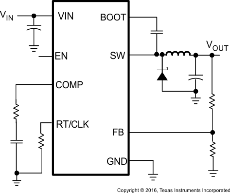
Simplified Schematic

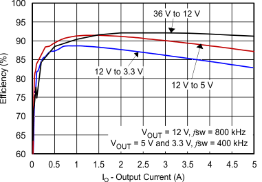
Efficiency vs Load Current
