SLVSFN6 December 2020 TPS54622-EP
PRODUCTION DATA
- 1 Features
- 2 Applications
- 3 Description
- 4 Revision History
- 5 Pin Configurations and Functions
- 6 Specifications
-
7 Detailed Description
- 7.1 Overview
- 7.2 Functional Block Diagram
- 7.3
Feature Description
- 7.3.1 Fixed-Frequency PWM Control
- 7.3.2 Continuous Current Mode Operation (CCM)
- 7.3.3 VIN and Power VIN Pins (VIN and PVIN)
- 7.3.4 Voltage Reference
- 7.3.5 Adjusting the Output Voltage
- 7.3.6 Safe Start-Up Into Prebiased Outputs
- 7.3.7 Error Amplifier
- 7.3.8 Slope Compensation
- 7.3.9 Enable and Adjusting Undervoltage Lockout
- 7.3.10 Adjustable Switching Frequency and Synchronization (RT/CLK)
- 7.3.11 Slow Start (SS/TR)
- 7.3.12 Power Good (PWRGD)
- 7.3.13 Output Overvoltage Protection (OVP)
- 7.3.14 Overcurrent Protection
- 7.3.15 Thermal Shutdown
- 7.3.16 Small Signal Model for Loop Response
- 7.3.17 Simple Small Signal Model for Peak Current Mode Control
- 7.3.18 Small Signal Model for Frequency Compensation
- 7.4 Device Functional Modes
-
8 Application and Implementation
- 8.1 Application Information
- 8.2
Typical Application
- 8.2.1 Design Requirements
- 8.2.2
Detailed Design Procedures
- 8.2.2.1 Custom Design With WEBENCH® Tools
- 8.2.2.2 Operating Frequency
- 8.2.2.3 Output Inductor Selection
- 8.2.2.4 Output Capacitor Selection
- 8.2.2.5 Input Capacitor Selection
- 8.2.2.6 Slow-Start Capacitor Selection
- 8.2.2.7 Bootstrap Capacitor Selection
- 8.2.2.8 Undervoltage Lockout Setpoint
- 8.2.2.9 Output Voltage Feedback Resistor Selection
- 8.2.2.10 Compensation Component Selection
- 8.2.2.11 Fast Transient Considerations
- 8.2.3 Application Curves
- 9 Power Supply Recommendations
- 10Layout
- 11Device and Documentation Support
- 12Mechanical, Packaging, and Orderable Information
Package Options
Mechanical Data (Package|Pins)
- RHL|14
Thermal pad, mechanical data (Package|Pins)
Orderable Information
6.6 Typical Characteristics
 Figure 6-1 High-Side RDS(on) vs Temperature
 Figure 6-3 Voltage Reference vs Temperature
 Figure 6-5 Shutdown Quiescent Current vs Temperature
 Figure 6-7 EN Pin Pullup Current vs Temperature
 Figure 6-9 Non-Switching Operating Quiescent Current vs Temperature
 Figure 6-11 (SS/TR - VSENSE) Offset vs Temperature
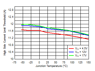
 Figure 6-13 High-Side Current Limit Threshold vs Temperature
 Figure 6-15 Minimum Controllable Duty Ratio vs Temperature
 Figure 6-17 Overcurrent Threshold vs Input Voltage.
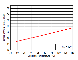
  Figure 6-2 Low-Side RDS(on) vs Temperature
 Figure 6-4 Oscillator Frequency vs Temperature
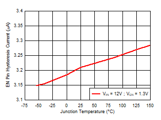
 Figure 6-6 EN Pin Hysteresis Current vs Temperature
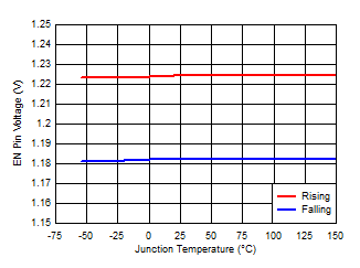
 Figure 6-8 EN Pin UVLO Threshold vs Temperature
 Figure 6-10 Slow Start Charge Current vs Temperature
 Figure 6-12 PWRGD Threshold vs Temperature
 Figure 6-14 Minimum Controllable On-Time vs Temperature
 Figure 6-16 BOOT-PH UVLO Threshold vs Temperature