SLVSFN6 December 2020 TPS54622-EP
PRODUCTION DATA
- 1 Features
- 2 Applications
- 3 Description
- 4 Revision History
- 5 Pin Configurations and Functions
- 6 Specifications
-
7 Detailed Description
- 7.1 Overview
- 7.2 Functional Block Diagram
- 7.3
Feature Description
- 7.3.1 Fixed-Frequency PWM Control
- 7.3.2 Continuous Current Mode Operation (CCM)
- 7.3.3 VIN and Power VIN Pins (VIN and PVIN)
- 7.3.4 Voltage Reference
- 7.3.5 Adjusting the Output Voltage
- 7.3.6 Safe Start-Up Into Prebiased Outputs
- 7.3.7 Error Amplifier
- 7.3.8 Slope Compensation
- 7.3.9 Enable and Adjusting Undervoltage Lockout
- 7.3.10 Adjustable Switching Frequency and Synchronization (RT/CLK)
- 7.3.11 Slow Start (SS/TR)
- 7.3.12 Power Good (PWRGD)
- 7.3.13 Output Overvoltage Protection (OVP)
- 7.3.14 Overcurrent Protection
- 7.3.15 Thermal Shutdown
- 7.3.16 Small Signal Model for Loop Response
- 7.3.17 Simple Small Signal Model for Peak Current Mode Control
- 7.3.18 Small Signal Model for Frequency Compensation
- 7.4 Device Functional Modes
-
8 Application and Implementation
- 8.1 Application Information
- 8.2
Typical Application
- 8.2.1 Design Requirements
- 8.2.2
Detailed Design Procedures
- 8.2.2.1 Custom Design With WEBENCH® Tools
- 8.2.2.2 Operating Frequency
- 8.2.2.3 Output Inductor Selection
- 8.2.2.4 Output Capacitor Selection
- 8.2.2.5 Input Capacitor Selection
- 8.2.2.6 Slow-Start Capacitor Selection
- 8.2.2.7 Bootstrap Capacitor Selection
- 8.2.2.8 Undervoltage Lockout Setpoint
- 8.2.2.9 Output Voltage Feedback Resistor Selection
- 8.2.2.10 Compensation Component Selection
- 8.2.2.11 Fast Transient Considerations
- 8.2.3 Application Curves
- 9 Power Supply Recommendations
- 10Layout
- 11Device and Documentation Support
- 12Mechanical, Packaging, and Orderable Information
Package Options
Mechanical Data (Package|Pins)
- RHL|14
Thermal pad, mechanical data (Package|Pins)
Orderable Information
3 Description
The TPS54622-EP device in thermally enhanced 3.5-mm × 3.5-mm VQFN package is a full-featured 17-V, 6-A synchronous step-down converter optimized for small designs through high efficiency and integrating the high-side and low-side MOSFETs. Further space savings are achieved through current mode control, which reduces component count, and by selecting a high switching frequency, reducing the footprint of the inductor.
The output voltage start-up ramp is controlled by the SS/TR pin, which allows operation as either a stand-alone power supply or in tracking situations. Power sequencing is also possible by correctly configuring the enable and the open-drain power good pins.
Cycle-by-cycle current limiting on the high-side FET protects the device in overload situations and is enhanced by a low-side sourcing current limit that prevents current runaway. There is also a low-side sinking current limit that turns off the low-side MOSFET to prevent excessive reverse current. Hiccup protection is triggered if the overcurrent condition has persisted for longer than the preset time. Thermal hiccup protection disables the device when the die temperature exceeds the thermal shutdown temperature and enables the part again after the built-in thermal shutdown hiccup time.
| PART NUMBER | PACKAGE(1) | BODY SIZE (NOM) |
|---|---|---|
| TPS54622-EP | VQFN (14) | 3.50 mm × 3.50 mm |
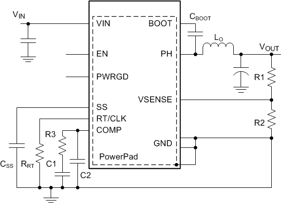
 Simplified Schematic
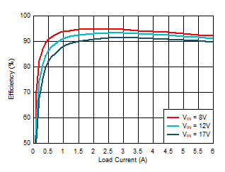
 Efficiency vs Load Current