SLVSC33A August 2013 – October 2022 TPS54625
PRODUCTION DATA
- 1 FEATURES
- 2 APPLICATIONS
- 3 DESCRIPTION
- 4 ORDERING INFORMATION (1)
- 5 ABSOLUTE MAXIMUM RATINGS
- 6 THERMAL INFORMATION
- 7 RECOMMENDED OPERATING CONDITIONS
- 8 ELECTRICAL CHARACTERISTICS
- 9 DEVICE INFORMATION
- 10OVERVIEW
- 11DETAILED DESCRIPTION
- 12TYPICAL CHARACTERISTICS
- 13DESIGN GUIDE
- 14THERMAL INFORMATION
- 15LAYOUT CONSIDERATIONS
- 16Revision History
Package Options
Mechanical Data (Package|Pins)
- PWP|14
Thermal pad, mechanical data (Package|Pins)
Orderable Information
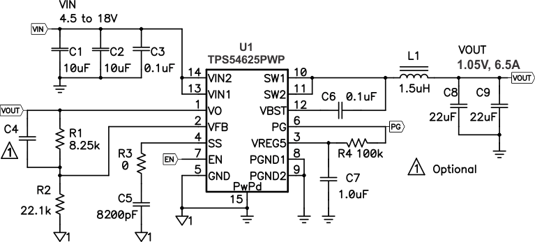
13.1 Step By Step Design Procedure
To begin the design process, you must know a few application parameters:
- Input voltage range
- Output voltage
- Output current
- Output voltage ripple
- Input voltage ripple
 Figure 13-1 Schematic