SLVSH95 July 2024 TPS546C25
ADVANCE INFORMATION
- 1
- 1 Features
- 2 Applications
- 3 Description
- 4 Pin Configuration and Functions
- 5 Specifications
-
6 Detailed Description
- 6.1 Overview
- 6.2 Functional Block Diagram
- 6.3
Feature Description
- 6.3.1 D-CAP4 Control
- 6.3.2 Internal VCC LDO and Using an External Bias on VCC Pin and VDRV Pin
- 6.3.3 Input Undervoltage Lockout (UVLO)
- 6.3.4 Differential Remote Sense and Internal, External Feedback Divider
- 6.3.5 Set the Output Voltage and VORST#
- 6.3.6 Start-Up and Shutdown
- 6.3.7 Dynamic Voltage Slew Rate
- 6.3.8 Set Switching Frequency
- 6.3.9 Switching Node (SW)
- 6.3.10 Overcurrent Limit and Low-side Current Sense
- 6.3.11 Negative Overcurrent Limit
- 6.3.12 Zero-Crossing Detection
- 6.3.13 Input Overvoltage Protection
- 6.3.14 Output Overvoltage and Undervoltage Protection
- 6.3.15 Overtemperature Protection
- 6.3.16 Telemetry
- 6.4 Device Functional Modes
- 6.5 Programming
-
7 Register Maps
- 7.1 Conventions for Documenting Block Commands
- 7.2 (01h) OPERATION
- 7.3 (02h) ON_OFF_CONFIG
- 7.4 (03h) CLEAR_FAULTS
- 7.5 (04h) PHASE
- 7.6 (09h) P2_PLUS_WRITE
- 7.7 (0Ah) P2_PLUS_READ
- 7.8 (0Eh) PASSKEY
- 7.9 (10h) WRITE_PROTECT
- 7.10 (15h) STORE_USER_ALL
- 7.11 (16h) RESTORE_USER_ALL
- 7.12 (19h) CAPABILITY
- 7.13 (1Bh) SMBALERT_MASK
- 7.14 (20h) VOUT_MODE
- 7.15 (21h) VOUT_COMMAND
- 7.16 (22h) VOUT_TRIM
- 7.17 (24h) VOUT_MAX
- 7.18 (25h) VOUT_MARGIN_HIGH
- 7.19 (26h) VOUT_MARGIN_LOW
- 7.20 (27h) VOUT_TRANSITION_RATE
- 7.21 (29h) VOUT_SCALE_LOOP
- 7.22 (2Ah) VOUT_SCALE_MONITOR
- 7.23 (2Bh) VOUT_MIN
- 7.24 (33h) FREQUENCY_SWITCH
- 7.25 (35h) VIN_ON
- 7.26 (36h) VIN_OFF
- 7.27 (39h) IOUT_CAL_OFFSET
- 7.28 (40h) VOUT_OV_FAULT_LIMIT
- 7.29 (41h) VOUT_OV_FAULT_RESPONSE
- 7.30 (42h) VOUT_OV_WARN_LIMIT
- 7.31 (43h) VOUT_UV_WARN_LIMIT
- 7.32 (44h) VOUT_UV_FAULT_LIMIT
- 7.33 (45h) VOUT_UV_FAULT_RESPONSE
- 7.34 (46h) IOUT_OC_FAULT_LIMIT
- 7.35 (48h) IOUT_OC_LV_FAULT_LIMIT
- 7.36 (49h) IOUT_OC_LV_FAULT_RESPONSE
- 7.37 (4Ah) IOUT_OC_WARN_LIMIT
- 7.38 (4Fh) OT_FAULT_LIMIT
- 7.39 (50h) OT_FAULT_RESPONSE
- 7.40 (51h) OT_WARN_LIMIT
- 7.41 (55h) VIN_OV_FAULT_LIMIT
- 7.42 (60h) TON_DELAY
- 7.43 (61h) TON_RISE
- 7.44 (64h) TOFF_DELAY
- 7.45 (65h) TOFF_FALL
- 7.46 (78h) STATUS_BYTE
- 7.47 (79h) STATUS_WORD
- 7.48 (7Ah) STATUS_VOUT
- 7.49 (7Bh) STATUS_IOUT
- 7.50 (7Ch) STATUS_INPUT
- 7.51 (7Dh) STATUS_TEMPERATURE
- 7.52 (7Eh) STATUS_CML
- 7.53 (7Fh) STATUS_OTHER
- 7.54 (80h) STATUS_MFR_SPECIFIC
- 7.55 (88h) READ_VIN
- 7.56 (8Bh) READ_VOUT
- 7.57 (8Ch) READ_IOUT
- 7.58 (8Dh) READ_TEMPERATURE_1
- 7.59 (98h) PMBUS_REVISION
- 7.60 (99h) MFR_ID
- 7.61 (9Ah) MFR_MODEL
- 7.62 (9Bh) MFR_REVISION
- 7.63 (ADh) IC_DEVICE_ID
- 7.64 (AEh) IC_DEVICE_REV
- 7.65 (D1h) SYS_CFG_USER1
- 7.66 (D2h) PMBUS_ADDR
- 7.67 (D4h) COMP
- 7.68 (D5h) VBOOT_OFFSET_1
- 7.69 (D6h) STACK_CONFIG
- 7.70 (D8h) PIN_DETECT_OVERRIDE
- 7.71 (D9h) NVM_CHECKSUM
- 7.72 (DAh) READ_TELEMETRY
- 7.73 (79h) STATUS_ALL
- 7.74 (DDh) EXT_WRITE_PROTECTION
- 7.75 (A4h) IMON_CAL
- 7.76 (FCh) FUSION_ID0
- 7.77 (FDh) FUSION_ID1
- 8 Application and Implementation
- 9 Device and Documentation Support
- 10Revision History
- 11Mechanical, Packaging, and Orderable Information
Package Options
Mechanical Data (Package|Pins)
- VBD|33
Thermal pad, mechanical data (Package|Pins)
Orderable Information
4 Pin Configuration and Functions
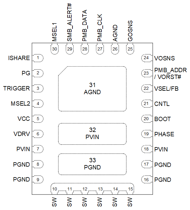
 Figure 4-1 VBD 33-pin WQFN Package (Top View)
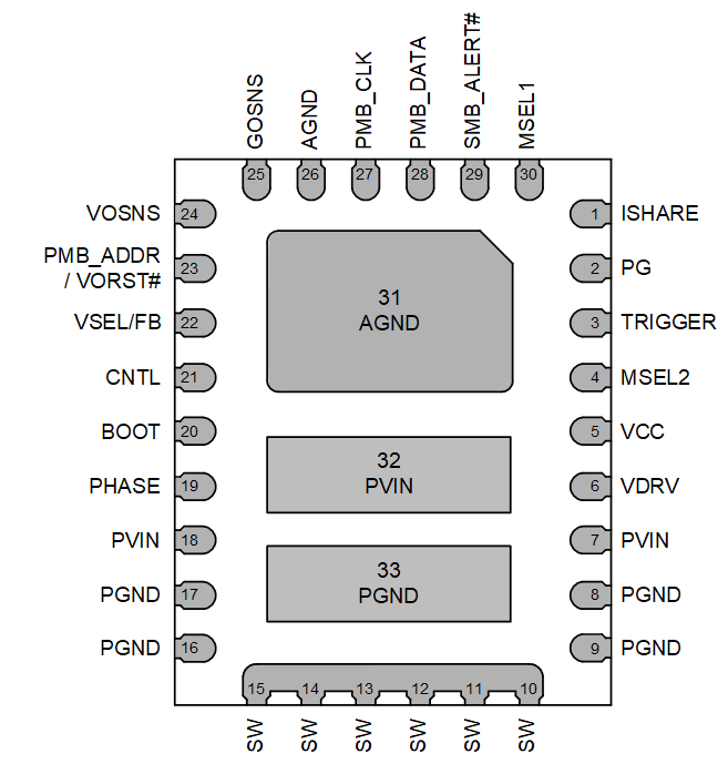
 Figure 4-2 VBD 33-pin WQFN Package (Bottom View)
Table 4-1 Pin Functions
| PIN | TYPE(1) | DESCRIPTION | |
|---|---|---|---|
| NAME | NO. | ||
| AGND | 26, 31 | G | Ground pin, reference point for internal control circuitry. |
| BOOT | 20 | P | Supply rail for the high-side gate driver (boost terminal). Connect the bootstrap capacitor from this pin to PHASE pin. A high temperature (X7R) 0.1μF or greater value ceramic capacitor is recommended. |
| CNTL | 21 | I | CTRL pin, an active-high input pin that, when asserted high, causes the converter to begin the soft-start sequence for the output voltage rail. |
| GOSNS | 25 | I | Negative input of the differential remote sense circuit, connect to the ground sense point on the load side. |
| ISHARE | 1 | I/O | ISHARE pin for stackable configuration. Tie this pin to other ISHARE pins in the stack. Do not connect (float) in standalone configuration. |
| MSEL1 | 30 | I | Use a resistor to AGND to select options for the device. See Pin Strapping. |
| MSEL2 | 4 | I | Use a resistor to AGND to select configuration options for the device. See Pin Strapping. |
| PG | 2 | O | Open-drain power-good indicator. |
| PGND | 8, 9, 16, 17, 33 | G | Power ground for the internal power stage. |
| PHASE | 19 | I/O | Return for high-side MOSFET driver. Shorted to SW internally. Connect the bootstrap capacitor from BOOT pin to PHASE pin. |
| PMB_ADDR/VORST# | 23 | I | The PMBus address, Primary or Secondary, Internal or External Feedback, Over-current Limit, Soft-start, and Fault Response can be set by tying an external resistor between this pin and AGND. See Pin Strapping. |
| PMB_CLK | 27 | I | PMBus clock pin, open drain. |
| PMB_DATA | 28 | I/O | PMBus bi-directional data pin, open drain. |
| PVIN | 7, 18, 32 | P | Power input for both the power stage and the input of the internal VCC LDO. |
| SMB_ALERT_# | 29 | O | SMBALERT# as described in the SMBus specification. The pin is open-drain. The SMBALERT# indicator is used in conjunction with the Alert Response Address (ARA). During nominal operation, the SMBALERT# is held high. |
| SW | 10–15 | O | Output switching terminal of the power converter. Connect these pins to the output inductor. |
| TRIGGER | 3 | I/O | TRIGGER pin for stackable configuration. Tie this pin to other TRIGGER pins in the stack. Do not connect (float) in standalone configuration. |
| VCC | 5 | P | Supply for analog control circuitry. Connect a 1Ohm resistor from VDRV to this pin and bypass with a 2.2μF capacitor to AGND. Check layout guidelines for more details. |
| VDRV | 6 | — | Internal 5V regulator output and internal connection to the gate drivers. An external 5V bias can be connected to this pin to save the power losses on the internal LDO. A 2.2μF (or 4.7μF), at least 6.3V rating ceramic capacitor is required to be placed from VDRV pin to PGND pins to decouple the noise generated by driver circuitry. Check layout guidelines for more details. |
| VOSNS | 24 | I | This pin is VOSNS and is the positive input of the differential remote sense circuit, connect to the Vout sense point on the load side. |
| VSEL/FB | 22 | I | When the device is configured to use the internal FB divider, this pin is VSEL. Use a resistor to AGND to select the output voltage. See Table TBD. When the device is configured for an external resister divider, this pin is the feedback pin of the device. Connect this pin to the midpoint of a resistor divider to set the output voltage. |
(1) I = Input, O = Output, I/O = Input or Output, G = Ground, P = Power.