SNVSBC5A December 2020 – December 2022 TPS548B28
PRODUCTION DATA
- 1 Features
- 2 Applications
- 3 Description
- 4 Revision History
- 5 Pin Configuration and Functions
- 6 Specifications
-
7 Detailed Description
- 7.1 Overview
- 7.2 Functional Block Diagram
- 7.3
Feature Description
- 7.3.1 Internal VCC LDO And Using External Bias On VCC Pin
- 7.3.2 Enable
- 7.3.3 Output Voltage Setting
- 7.3.4 Internal Fixed Soft Start and External Adjustable Soft Start
- 7.3.5 External REFIN For Output Voltage Tracking
- 7.3.6 Frequency and Operation Mode Selection
- 7.3.7 D-CAP3™ Control Mode
- 7.3.8 Low-side FET Zero-Crossing
- 7.3.9 Current Sense and Positive Overcurrent Protection
- 7.3.10 Low-side FET Negative Current Limit
- 7.3.11 Power Good
- 7.3.12 Overvoltage and Undervoltage Protection
- 7.3.13 Out-Of-Bounds (OOB) Operation
- 7.3.14 Output Voltage Discharge
- 7.3.15 UVLO Protection
- 7.3.16 Thermal Shutdown
- 7.4 Device Functional Modes
-
8 Application and Implementation
- 8.1 Application Information
- 8.2
Typical Application
- 8.2.1 Design Requirements
- 8.2.2
Detailed Design Procedure
- 8.2.2.1 Output Voltage Setting Point
- 8.2.2.2 Choose the Switching Frequency and the Operation Mode
- 8.2.2.3 Choose the Inductor
- 8.2.2.4 Set the Current Limit (TRIP)
- 8.2.2.5 Choose the Output Capacitor
- 8.2.2.6 Choose the Input Capacitors (CIN)
- 8.2.2.7 Soft Start Capacitor (SS/REFIN Pin)
- 8.2.2.8 EN Pin Resistor Divider
- 8.2.2.9 VCC Bypass Capacitor
- 8.2.2.10 BOOT Capacitor
- 8.2.2.11 PGOOD Pullup Resistor
- 8.2.3 Application Curves
- 8.3 Power Supply Recommendations
- 8.4 Layout
- 9 Device and Documentation Support
- 10Mechanical, Packaging, and Orderable Information
Package Options
Mechanical Data (Package|Pins)
- RWW|21
Thermal pad, mechanical data (Package|Pins)
Orderable Information
7.4.4 Powering the Device From a 3.3-V Bus
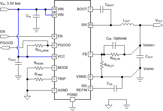
The device can also work for up to a 20-A load current when powering from a 3.3-V bus with a single VIN configuration. To ensure the internal analog circuitry and the gate drives are powered up properly, VCC pin must be shorted to VIN pins with low impedance trace. A trace with at least 24-mil width is recommended. A 2.2-µF, at least 6.3-V rating, VCC-to-PGND decoupling capacitor is still recommended to be placed as close as possible to VCC pin. Due to the maximum rating limit on VCC pin, the VIN input range under this configuration is 3 V to 3.6 V. The input voltage must stay higher than both VIN UVLO and VCC UVLO, otherwise the device will shut down immediately. Figure 7-6 shows an example for this single VIN configuration.
VIN and EN are the two signals to enable the part. For start-up sequence, any sequence between the VIN and EN signals can power the device up correctly.
 Figure 7-6 Single VIN Configuration For 3.3-V Bus