SLUSC70D March 2016 – July 2017 TPS548D22
PRODUCTION DATA.
- 1 Features
- 2 Applications
- 3 Description
- 4 Revision History
- 5 Pin Configuration and Functions
- 6 Specifications
-
7 Detailed Description
- 7.1 Overview
- 7.2 Functional Block Diagram
- 7.3 Feature Description
- 7.4 Device Functional Modes
- 7.5 Programming
-
8 Application and Implementation
- 8.1 Application Information
- 8.2
Typical Applications
- 8.2.1 TPS548D22 1.5-V to 16-V Input, 1-V Output, 40-A Converter
- 8.2.2 Design Requirements
- 8.2.3
Design Procedure
- 8.2.3.1 Switching Frequency Selection
- 8.2.3.2 Inductor Selection
- 8.2.3.3 Output Capacitor Selection
- 8.2.3.4 Input Capacitor Selection
- 8.2.3.5 Bootstrap Capacitor Selection
- 8.2.3.6 BP Pin
- 8.2.3.7 R-C Snubber and VIN Pin High-Frequency Bypass
- 8.2.3.8 Optimize Reference Voltage (VSEL)
- 8.2.3.9 MODE Pin Selection
- 8.2.3.10 Overcurrent Limit Design.
- 8.2.4 Application Curves
- 9 Power Supply Recommendations
- 10Layout
- 11Device and Documentation Support
- 12Mechanical, Packaging, and Orderable Information
Package Options
Mechanical Data (Package|Pins)
- RVF|40
Thermal pad, mechanical data (Package|Pins)
- RVF|40
Orderable Information
7.3.7.1 Current Limit (ILIM) Functionality
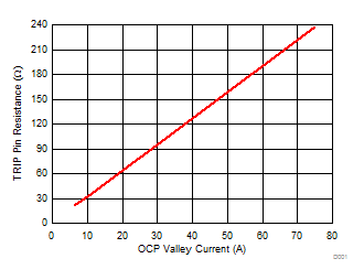
 Figure 15. Current Limit Resistance vs OCP Valley Overcurrent Limit
The ILIM pin sets the OCP level. Connect the ILIM pin to GND through the voltage setting resistor, RILIM. In order to provide both good accuracy and cost effective solution, TPS548D22 device supports temperature compensated internal MOSFET RDS(on) sensing.
Also, the TPS548D22 device performs both positive and negative inductor current limiting with the same magnitudes. The positive current limit normally protects the inductor from saturation that causes damage to the high-side FET and low-side FET. The negative current limit protects the low-side FET during OVP discharge.
The voltage between GND pin and SW pin during the OFF time monitors the inductor current. The current limit has 3000 ppm/°C temperature slope to compensate the temperature dependency of the on-resistance (RDS(on)). The GND pin is used as the positive current sensing node.
TPS548D22 device uses cycle-by-cycle over-current limiting control. The inductor current is monitored during the OFF state and the controller maintains the OFF state during the period that the inductor current is larger than the overcurrent ILIM level. VILIM sets the valley level of the inductor current.