SLVSES4D September 2019 – June 2024 TPS54J060
PRODUCTION DATA
- 1
- 1 Features
- 2 Applications
- 3 Description
- 4 Pin Configuration and Functions
- 5 Specifications
-
6 Detailed Description
- 6.1 Overview
- 6.2 Functional Block Diagram
- 6.3
Feature Description
- 6.3.1 Enable and Internal LDO
- 6.3.2 Split Rail and External LDO
- 6.3.3 Output Voltage Setting
- 6.3.4 Soft Start and Output-Voltage Tracking
- 6.3.5 Frequency and Operation Mode Selection
- 6.3.6 D-CAP3™ Control Mode
- 6.3.7 Current Sense and Positive Overcurrent Protection
- 6.3.8 Low-side FET Negative Current Limit
- 6.3.9 Power Good
- 6.3.10 Overvoltage and Undervoltage Protection
- 6.3.11 Out-Of-Bounds Operation (OOB)
- 6.3.12 Output Voltage Discharge
- 6.3.13 UVLO Protection
- 6.3.14 Thermal Shutdown
- 6.4 Device Functional Modes
-
7 Application and Implementation
- 7.1 Application Information
- 7.2
Typical Application
- 7.2.1 Design Requirements
- 7.2.2
Detailed Design Procedure
- 7.2.2.1 Choose the Switching Frequency and Operation Mode (MODE Pin)
- 7.2.2.2 Choose the Output Inductor (L)
- 7.2.2.3 Set the Current Limit (TRIP)
- 7.2.2.4 Choose the Output Capacitors (COUT)
- 7.2.2.5 Choose the Input Capacitors (CIN)
- 7.2.2.6 Feedback Network (FB Pin)
- 7.2.2.7 Soft Start Capacitor (SS/REFIN Pin)
- 7.2.2.8 EN Pin Resistor Divider
- 7.2.2.9 VCC Bypass Capacitor
- 7.2.2.10 BOOT Capacitor
- 7.2.2.11 Series BOOT Resistor and RC Snubber
- 7.2.2.12 PGOOD Pullup Resistor
- 7.2.3 Application Curves
- 7.3 Power Supply Recommendations
- 7.4 Layout
- 8 Device and Documentation Support
- 9 Revision History
- 10Mechanical, Packaging, and Ordering Information
Package Options
Mechanical Data (Package|Pins)
- RPG|14
Thermal pad, mechanical data (Package|Pins)
Orderable Information
4 Pin Configuration and Functions
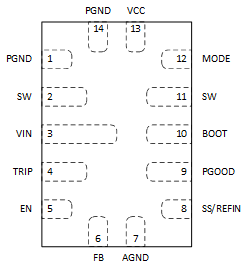
 Figure 4-1 14-Pin VQFN-HR, RPG
Package (Top View)
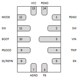
 Figure 4-2 14-Pin VQFN-HR, RPG
Package (Bottom View)
Figure 4-2 14-Pin VQFN-HR, RPG
Package (Bottom View)Table 4-1 Pin Functions
| PIN | TYPE(1) | DESCRIPTION | |
|---|---|---|---|
| NO. | NAME | ||
| 1, 14 | PGND | G | Power ground of internal low-side MOSFET |
| 2., 11 | SW | O | Output switching terminal of the power converter. Connect this pin to the output inductor. |
| 3 | VIN | I | Power-supply input pins for both integrated power MOSFET pair and the internal regulator. Place the decoupling input capacitors as close as possible to VIN pins. |
| 4 | TRIP | I/O | Current limit setting pin. Connect a resistor to ground to set the current limit trip point. See Section 6.3.7 for detailed OCP setting. |
| 5 | EN | I | Enable pin. The enable pin turns the DC/DC switching converter on or off. Floating the EN pin is not recommended. |
| 6 | FB | I | Output feedback input. A resistor divider from the VOUT to AGND (tapped to FB pin) sets the output voltage. |
| 7 | AGND | G | Analog ground pin, reference point for internal control circuits |
| 8 | SS/REFIN | I/O | Internal reference voltage can be overridden by an external voltage source on this pin for tracking application. Connecting a capacitor to AGND increases soft-start time. |
| 9 | PGOOD | O | Open-drain power-good status signal. A high voltage indicates the FB voltage has moved inside the specified limits. |
| 10 | BOOT | I/O | Supply rail for the high-side gate driver (boost terminal). Connect the bootstrap capacitor from this pin to SW node. |
| 12 | MODE | I | The MODE pin sets the forced continuous-conduction mode (FCCM) or skip-mode operation. It also selects the operating frequency. |
| 13 | VCC | I/O | Internal 3-V LDO output. An external bias with 3.3-V ±5% voltage can be connected to this pin to save the power losses on the internal LDO. The voltage source on this pin powers both the internal circuitry and gate driver. For the decoupling, suggest a 1-µF ceramic capacitor as close to VCC pin as possible. |
(1) I = Input, O = Output, P = Supply, G = Ground