SLVSES4D September 2019 – June 2024 TPS54J060
PRODUCTION DATA
- 1
- 1 Features
- 2 Applications
- 3 Description
- 4 Pin Configuration and Functions
- 5 Specifications
-
6 Detailed Description
- 6.1 Overview
- 6.2 Functional Block Diagram
- 6.3
Feature Description
- 6.3.1 Enable and Internal LDO
- 6.3.2 Split Rail and External LDO
- 6.3.3 Output Voltage Setting
- 6.3.4 Soft Start and Output-Voltage Tracking
- 6.3.5 Frequency and Operation Mode Selection
- 6.3.6 D-CAP3™ Control Mode
- 6.3.7 Current Sense and Positive Overcurrent Protection
- 6.3.8 Low-side FET Negative Current Limit
- 6.3.9 Power Good
- 6.3.10 Overvoltage and Undervoltage Protection
- 6.3.11 Out-Of-Bounds Operation (OOB)
- 6.3.12 Output Voltage Discharge
- 6.3.13 UVLO Protection
- 6.3.14 Thermal Shutdown
- 6.4 Device Functional Modes
-
7 Application and Implementation
- 7.1 Application Information
- 7.2
Typical Application
- 7.2.1 Design Requirements
- 7.2.2
Detailed Design Procedure
- 7.2.2.1 Choose the Switching Frequency and Operation Mode (MODE Pin)
- 7.2.2.2 Choose the Output Inductor (L)
- 7.2.2.3 Set the Current Limit (TRIP)
- 7.2.2.4 Choose the Output Capacitors (COUT)
- 7.2.2.5 Choose the Input Capacitors (CIN)
- 7.2.2.6 Feedback Network (FB Pin)
- 7.2.2.7 Soft Start Capacitor (SS/REFIN Pin)
- 7.2.2.8 EN Pin Resistor Divider
- 7.2.2.9 VCC Bypass Capacitor
- 7.2.2.10 BOOT Capacitor
- 7.2.2.11 Series BOOT Resistor and RC Snubber
- 7.2.2.12 PGOOD Pullup Resistor
- 7.2.3 Application Curves
- 7.3 Power Supply Recommendations
- 7.4 Layout
- 8 Device and Documentation Support
- 9 Revision History
- 10Mechanical, Packaging, and Ordering Information
Package Options
Mechanical Data (Package|Pins)
- RPG|14
Thermal pad, mechanical data (Package|Pins)
Orderable Information
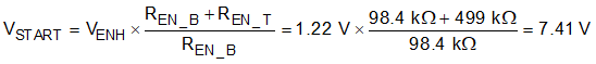
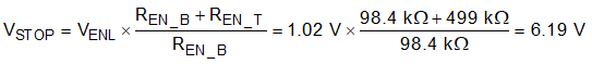
7.2.2.8 EN Pin Resistor Divider
A resistor divider on the EN pin can be used to increase the input voltage that the converter begins the start-up sequence. Increasing the input voltage the converter starts up at can be useful in high output voltage applications. The resistor divider can be selected so the converter starts switching after the input voltage is greater than the output voltage. If the output voltage comes up before the input voltage is sufficient, UVP can be tripped and cause the converter to latch off.
To set the start voltage, first select the bottom resistor (REN_B). The recommended value is between 1 kΩ and 100 kΩ. There is an internal pulldown resistance with a nominal value of 6 MΩ and this must be included for the most accurate calculations. This is especially important when the bottom resistor is a higher value, near 100 kΩ. This example uses a 100-kΩ resistor and this combined with the internal resistance in parallel results in an equivalent bottom resistance of 98.4 kΩ. The top resistor value for the target start voltage is calculated with Equation 29. In this example, the nearest standard value of 499 kΩ is selected for REN_T.

The start and stop voltages with the selected EN resistor divider can be calculated with Equation 28 and Equation 31.