SNVSBM9B July 2020 – November 2020 TPS54JB20
PRODUCTION DATA
- 1 Features
- 2 Applications
- 3 Description
- 4 Revision History
- 5 Pin Configuration and Functions
- 6 Specifications
-
7 Detailed Description
- 7.1 Overview
- 7.2 Functional Block Diagram
- 7.3
Feature Description
- 7.3.1 Internal VCC LDO And Using External Bias On VCC Pin
- 7.3.2 Enable
- 7.3.3 Output Voltage Setting
- 7.3.4 Internal Fixed Soft Start and External Adjustable Soft Start
- 7.3.5 External REFIN For Output Voltage Tracking
- 7.3.6 Frequency and Operation Mode Selection
- 7.3.7 D-CAP3 Control
- 7.3.8 Low-side FET Zero-Crossing
- 7.3.9 Current Sense and Positive Overcurrent Protection
- 7.3.10 Low-side FET Negative Current Limit
- 7.3.11 Power Good
- 7.3.12 Overvoltage and Undervoltage Protection
- 7.3.13 Out-Of-Bounds (OOB) Operation
- 7.3.14 Output Voltage Discharge
- 7.3.15 UVLO Protection
- 7.3.16 Thermal Shutdown
- 7.4 Device Functional Modes
-
8 Application and Implementation
- 8.1 Application Information
- 8.2
Typical Application
- 8.2.1 Design Requirements
- 8.2.2
Detailed Design Procedure
- 8.2.2.1 Output Voltage Setting Point
- 8.2.2.2 Choose the Switching Frequency and the Operation Mode
- 8.2.2.3 Choose the Inductor
- 8.2.2.4 Set the Current Limit (TRIP)
- 8.2.2.5 Choose the Output Capacitor
- 8.2.2.6 Choose the Input Capacitors (CIN)
- 8.2.2.7 Soft Start Capacitor (SS/REFIN Pin)
- 8.2.2.8 EN Pin Resistor Divider
- 8.2.2.9 VCC Bypass Capacitor
- 8.2.2.10 BOOT Capacitor
- 8.2.2.11 Series BOOT Resistor and RC Snubber
- 8.2.2.12 PGOOD Pullup Resistor
- 8.2.3 Application Curves
- 9 Power Supply Recommendations
- 10Layout
- 11Device and Documentation Support
- 12Mechanical, Packaging, and Orderable Information
Package Options
Mechanical Data (Package|Pins)
- RWW|21
Thermal pad, mechanical data (Package|Pins)
Orderable Information
8.2.2.5 Choose the Output Capacitor
There are three considerations for selecting the value of the output capacitor.
- Stability
- Steady state output voltage ripple
- Regulator transient response to a change load current


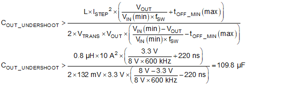
Equation 19 and Equation 20 calculate the minimum capacitance to meet the transient response requirement of 132 mV with a 10-A step. These equations calculate the necessary output capacitance to hold the output voltage steady while the inductor current ramps up or ramps down after a load step.


The output capacitance needed to meet the overshoot requirement is the highest value so this sets the required minimum output capacitance for this example. Stability requirements can also limit the maximum output capacitance and Equation 21 calculates the recommended maximum output capacitance. This calculation keeps the LC double pole above 1/100th the fSW. It can be possible to use more output capacitance but the stability must be checked through a bode plot or transient response measurement. The selected output capacitance is ceramic capacitors. When using ceramic capacitors, the capacitance must be derated due to DC and AC bias effects. The selected capacitors derate to their nominal value giving an effective total capacitance of 879.5 μF. This effective capacitance meets the minimum and maximum requirements.

This application uses all ceramic capacitors so the effects of ESR on the ripple and transient were ignored. If using non ceramic capacitors, as a starting point, the ESR should be below the values calculated in Equation 22 to meet the ripple requirement and Equation 23 to meet the transient requirement. For more accurate calculations or if using mixed output capacitors, the impedance of the output capacitors should be used to determine if the ripple and transient requirements can be met.

