SLIS132A October 2008 – March 2015 TPS55065-Q1
PRODUCTION DATA.
- 1 Features
- 2 Applications
- 3 Description
- 4 Revision History
- 5 Pin Configuration and Functions
- 6 Specifications
-
7 Detailed Description
- 7.1 Overview
- 7.2 Functional Block Diagram
- 7.3
Feature Description
- 7.3.1 Switched-Mode Input/Output Terminals (L1, L2)
- 7.3.2 Supply Terminal (Vdriver)
- 7.3.3 Internal Supply Decoupling Terminal (Vlogic)
- 7.3.4 Input Voltage Monitoring Terminal (AIN)
- 7.3.5 Input Undervoltage Alarm Terminal (AOUT)
- 7.3.6 Reset Delay Timer Terminal (REST)
- 7.3.7 Reset Terminal (RESET)
- 7.3.8 Main Regulator Output Terminal (VOUT)
- 7.3.9 Low-Power-Mode Terminal (CLP)
- 7.3.10 Switch-Output Terminal (5Vg)
- 7.3.11 5Vg-Enable Terminal (5Vg_ENABLE)
- 7.3.12 Slew-Rate Control Terminals (SCR0, SCR1)
- 7.3.13 Modulator Frequency Setting (Terminal Rmod)
- 7.3.14 Ground Terminal (PGND)
- 7.3.15 Enable Terminal (ENABLE)
- 7.3.16 Bootstrap Terminals (CBOOT1 and CBOOT2)
- 7.4 Device Functional Modes
- 8 Application and Implementation
- 9 Power Supply Recommendations
- 10Layout
- 11Device and Documentation Support
- 12Mechanical, Packaging, and Orderable Information
Package Options
Mechanical Data (Package|Pins)
- PWP|20
Thermal pad, mechanical data (Package|Pins)
- PWP|20
Orderable Information
8 Application and Implementation
NOTE
Information in the following applications sections is not part of the TI component specification, and TI does not warrant its accuracy or completeness. TI’s customers are responsible for determining suitability of components for their purposes. Customers should validate and test their design implementation to confirm system functionality.
8.1 Application Information
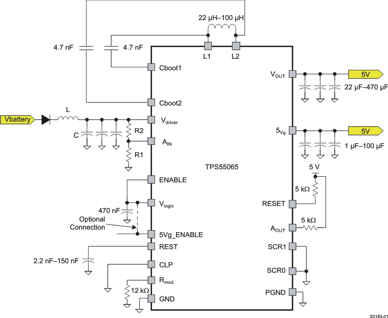
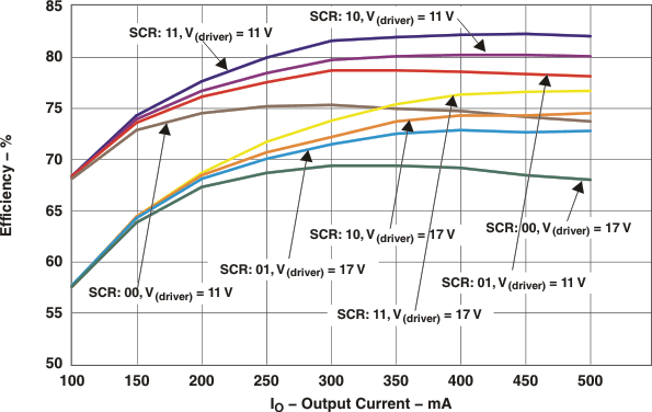
The TPS55065 can be operated in a buck boost configuration with voltage mode control. The device is capable of monitoring the output as well as the input supply rail. The device also offers a frequency modulation scheme for minimizing EMI. The slew rate is set using the SCR0 and the SCR1 terminals. The average converter efficiency varies with the different slew rate controls of the Q1 switching FET. These variations are demonstrated using this design example at an input voltage of 11 V and 17 V.
8.2 Typical Application

NOTE
When this attachment method is not implemented correctly, this product may operate inefficiently. Power dissipation capability may be adversely affected when the device is incorrectly mounted onto the circuit board.
8.2.1 Design Requirements
For this design example, use the parameters listed in Table 4 as the input parameters.
Table 4. Design Parameters
| DESIGN PARAMETERS | VALUE |
|---|---|
| Input voltage V(driver) | 11 V to 18 V |
| Output current (maximum) | 500 mA |
Four different SCRx settings will be used to analyze the difference in converter efficiency with variations in slew rate (see Figure 20). The Buck equations mentioned in Buck Mode will be used to calculate the rest of the design parameters.
8.2.2 Detailed Design Procedure
8.2.2.1 Buck Mode
- Select inductor ripple current ΔIL: for example, ΔIL = 0.2 × IOUT
- Calculate inductor L
- Inductor peak current
- Output voltage ripple

where


Usually, the first term is dominant.

Using the previous equations, with Vin (maximum) as 18 V, Vout as 5 V, fSW as 440 kHz, and Inductor ripple current of 0.1 A, the inductance is calculated to be 82.1 µH with inductor peak current as 0.55 A.
8.2.2.2 Boost Mode
- Select inductor ripple current ΔIL: for example ΔIL = 0.2 × IIN
- Calculate inductor L
- Inductor peak current
- Output voltage ripple

where


8.2.3 Application Curve
