SLVSHF9 august 2023 TPS552872-Q1
PRODUCTION DATA
- 1
- 1 Features
- 2 Applications
- 3 Description
- 4 Revision History
- 5 Pin Configuration and Functions
- 6 Specifications
-
7 Detailed Description
- 7.1 Overview
- 7.2 Functional Block Diagram
- 7.3
Feature Description
- 7.3.1 VCC Power Supply
- 7.3.2 EXTVCC Power Supply
- 7.3.3 Input Undervoltage Lockout
- 7.3.4 Enable and Programmable UVLO
- 7.3.5 Soft Start
- 7.3.6 Shutdown
- 7.3.7 Switching Frequency
- 7.3.8 Switching Frequency Dithering
- 7.3.9 Inductor Current Limit
- 7.3.10 Internal Charge Path
- 7.3.11 Output Voltage Setting
- 7.3.12 Output Current Monitoring and Cable Voltage Droop Compensation
- 7.3.13 Output Current Limit
- 7.3.14 Overvoltage Protection
- 7.3.15 Output Short Circuit Protection
- 7.3.16 Power Good
- 7.3.17 Constant Current Output Indication
- 7.3.18 Thermal Shutdown
- 7.4 Device Functional Modes
- 8 Application and Implementation
- 9 Device and Documentation Support
- 10Mechanical, Packaging, and Orderable Information
Package Options
Mechanical Data (Package|Pins)
- RYQ|21
Thermal pad, mechanical data (Package|Pins)
- RYQ|21
Orderable Information
7.3.7 Switching Frequency
The TPS552872-Q1 uses a fixed frequency average current control scheme. The switching frequency is between 200 kHz and 2.2 MHz set by placing a resistor at the FSW pin. An internal amplifier holds this pin at a fixed voltage of 1 V. The setting resistance is between maximum of 100 kΩ and minimum of 8.4 kΩ. Use Equation 3 to calculate the resistance by a given switching frequency.
where
- RFSW is the resistance at the FSW pin (Ω)
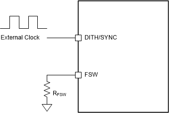
For noise-sensitive applications, the TPS552872-Q1 can be synchronized to an external clock signal applied to the DITH/SYNC pin. The duty cycle of the external clock is recommended in the range of 30% to 70%. A resistor also must be connected to the FSW pin when the TPS552872-Q1 is switching by the external clock. The external clock frequency at the DITH/SYNC pin must have lower than 0.4-V low level voltage and must be within ±30% of the corresponding frequency set by the resistor. Figure 7-3 is a recommended configuration.
 Figure 7-3 External Clock Configuration