SLVSFQ7A December 2020 – December 2021 TPS55288-Q1
PRODUCTION DATA
- 1 Features
- 2 Applications
- 3 Description
- 4 Revision History
- 5 Pin Configuration and Functions
- 6 Specifications
-
7 Detailed Description
- 7.1 Overview
- 7.2 Functional Block Diagram
- 7.3
Feature Description
- 7.3.1 VCC Power Supply
- 7.3.2 Operation Mode Setting
- 7.3.3 Input Undervoltage Lockout
- 7.3.4 Enable and Programmable UVLO
- 7.3.5 Soft Start
- 7.3.6 Shutdown and Load Discharge
- 7.3.7 Switching Frequency
- 7.3.8 Switching Frequency Dithering
- 7.3.9 Inductor Current Limit
- 7.3.10 Internal Charge Path
- 7.3.11 Output Voltage Setting
- 7.3.12 Output Current Monitoring and Cable Voltage Droop Compensation
- 7.3.13 Integrated Gate Drivers
- 7.3.14 Output Current Limit
- 7.3.15 Overvoltage Protection
- 7.3.16 Output Short Circuit Protection
- 7.3.17 Thermal Shutdown
- 7.4 Device Functional Modes
- 7.5 Programming
- 7.6
Register Maps
- 7.6.1 REF Register (Address = 0h, 1h) [reset = 11010010h, 00000000h]
- 7.6.2 IOUT_LIMIT Register (Address = 2h) [reset = 11100100h]
- 7.6.3 VOUT_SR Register (Address = 3h) [reset = 00000001h]
- 7.6.4 VOUT_FS Register (Address = 4h) [reset = 00000011h]
- 7.6.5 CDC Register (Address = 5h) [reset = 11100000h]
- 7.6.6 MODE Register (Address = 6h) [reset = 00100000h]
- 7.6.7 STATUS Register (Address = 7h) [reset = 00000011h]
- 7.6.8 Register Summary
- 8 Application and Implementation
- 9 Power Supply Recommendations
- 10Layout
- 11Device and Documentation Support
- 12Mechanical, Packaging, and Orderable Information
Package Options
Mechanical Data (Package|Pins)
- RPM|26
Thermal pad, mechanical data (Package|Pins)
- RPM|26
Orderable Information
3 Description
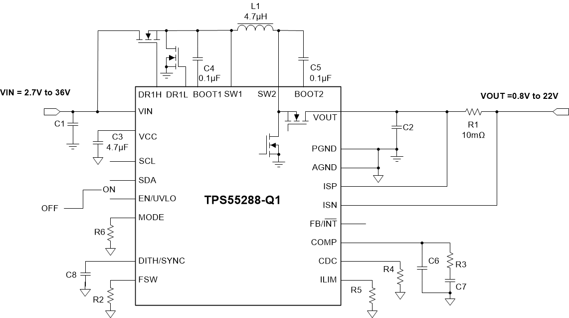
The TPS55288-Q1 is a synchronous four-switch buck-boost converter capable of regulating the output voltage at, above, or below the input voltage. The TPS55288-Q1 operates over 2.7-V to 36-V wide input voltage and is capable of outputing 0.8-V to 22-V voltage to support a variety of applications.
The TPS55288-Q1 integrates two 16-A MOSFETs of the boost leg to balance the solution size and efficiency. With the programmable output voltage and output current limit through I2C interface, the TPS55288-Q1 is fully compliant to the USB PD specification. The TPS55288-Q1 is capable of delivering 100 W from 12-V input voltage.
The TPS55288-Q1 employs an average current-mode control scheme. The switching frequency is programmable from 200 kHz to 2.2 MHz by an external resistor and can be synchronized to an external clock. The TPS55288-Q1 also provides optional spread spectrum to minimize peak EMI.
The TPS55288-Q1 offers output over-voltage protection, average inductor current limit, cycle-by-cycle peak current limit and output short circuit protection. The TPS55288-Q1 also ensures safe operating with optional output current limit and hiccup-mode protection in sustained overload conditions.
The TPS55288-Q1 can use a small inductor and small capacitors with high switching frequency. It is available in a 4.0-mm × 3.5-mm QFN package.
| PART NUMBER | PACKAGE(1) | BODY SIZE |
|---|---|---|
| TPS55288-Q1 | VQFN-HR | 4.00 mm × 3.50 mm |
 Typical Application
Circuit