SLVSFQ7A December 2020 – December 2021 TPS55288-Q1
PRODUCTION DATA
- 1 Features
- 2 Applications
- 3 Description
- 4 Revision History
- 5 Pin Configuration and Functions
- 6 Specifications
-
7 Detailed Description
- 7.1 Overview
- 7.2 Functional Block Diagram
- 7.3
Feature Description
- 7.3.1 VCC Power Supply
- 7.3.2 Operation Mode Setting
- 7.3.3 Input Undervoltage Lockout
- 7.3.4 Enable and Programmable UVLO
- 7.3.5 Soft Start
- 7.3.6 Shutdown and Load Discharge
- 7.3.7 Switching Frequency
- 7.3.8 Switching Frequency Dithering
- 7.3.9 Inductor Current Limit
- 7.3.10 Internal Charge Path
- 7.3.11 Output Voltage Setting
- 7.3.12 Output Current Monitoring and Cable Voltage Droop Compensation
- 7.3.13 Integrated Gate Drivers
- 7.3.14 Output Current Limit
- 7.3.15 Overvoltage Protection
- 7.3.16 Output Short Circuit Protection
- 7.3.17 Thermal Shutdown
- 7.4 Device Functional Modes
- 7.5 Programming
- 7.6
Register Maps
- 7.6.1 REF Register (Address = 0h, 1h) [reset = 11010010h, 00000000h]
- 7.6.2 IOUT_LIMIT Register (Address = 2h) [reset = 11100100h]
- 7.6.3 VOUT_SR Register (Address = 3h) [reset = 00000001h]
- 7.6.4 VOUT_FS Register (Address = 4h) [reset = 00000011h]
- 7.6.5 CDC Register (Address = 5h) [reset = 11100000h]
- 7.6.6 MODE Register (Address = 6h) [reset = 00100000h]
- 7.6.7 STATUS Register (Address = 7h) [reset = 00000011h]
- 7.6.8 Register Summary
- 8 Application and Implementation
- 9 Power Supply Recommendations
- 10Layout
- 11Device and Documentation Support
- 12Mechanical, Packaging, and Orderable Information
Package Options
Mechanical Data (Package|Pins)
- RPM|26
Thermal pad, mechanical data (Package|Pins)
- RPM|26
Orderable Information
8.2.3 Application Curves
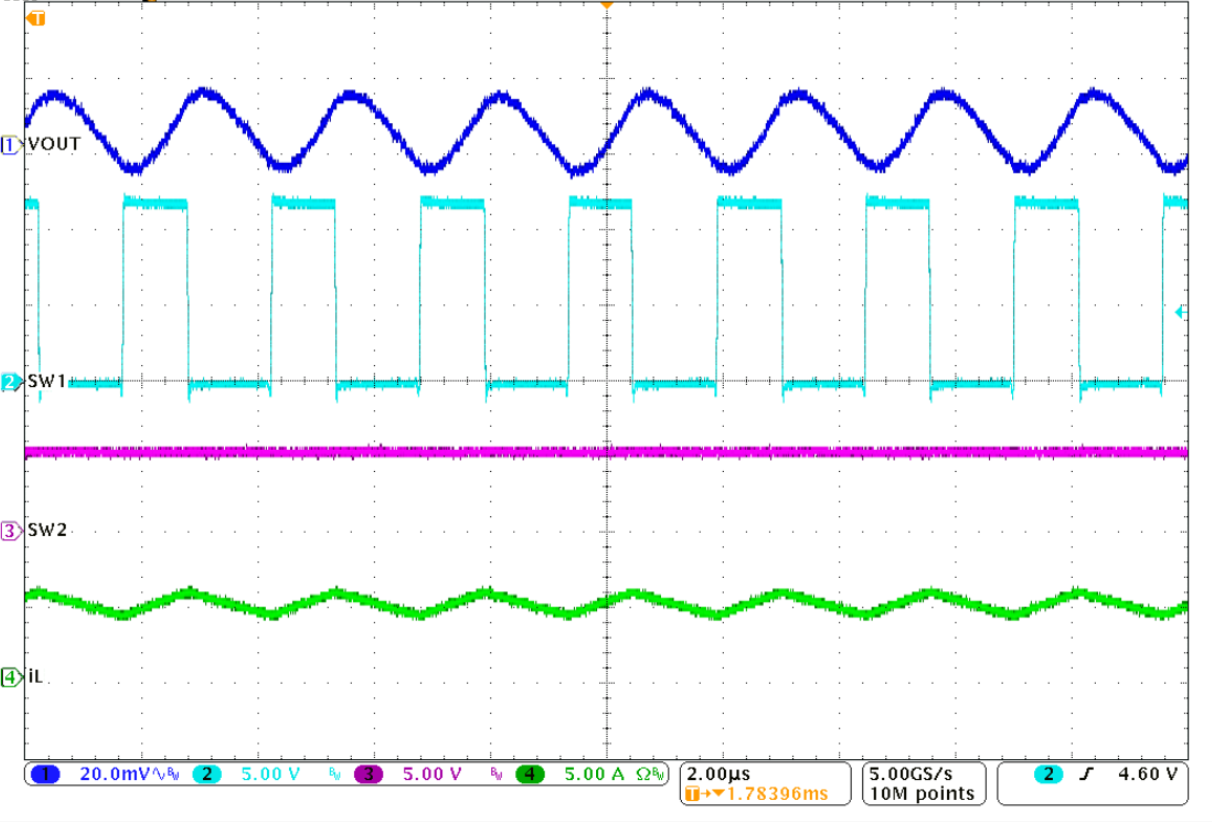 Figure 8-2 Switching Waveforms in VIN = 12 V, VOUT = 5 V,
IO = 5 A, FPWM
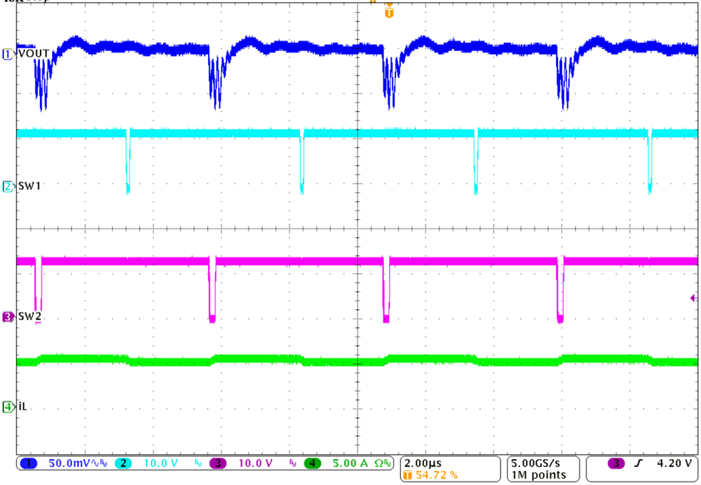 Figure 8-4 Switching Waveforms in
VIN = 12 V, VOUT = 12 V, IO = 5 A,
FPWM
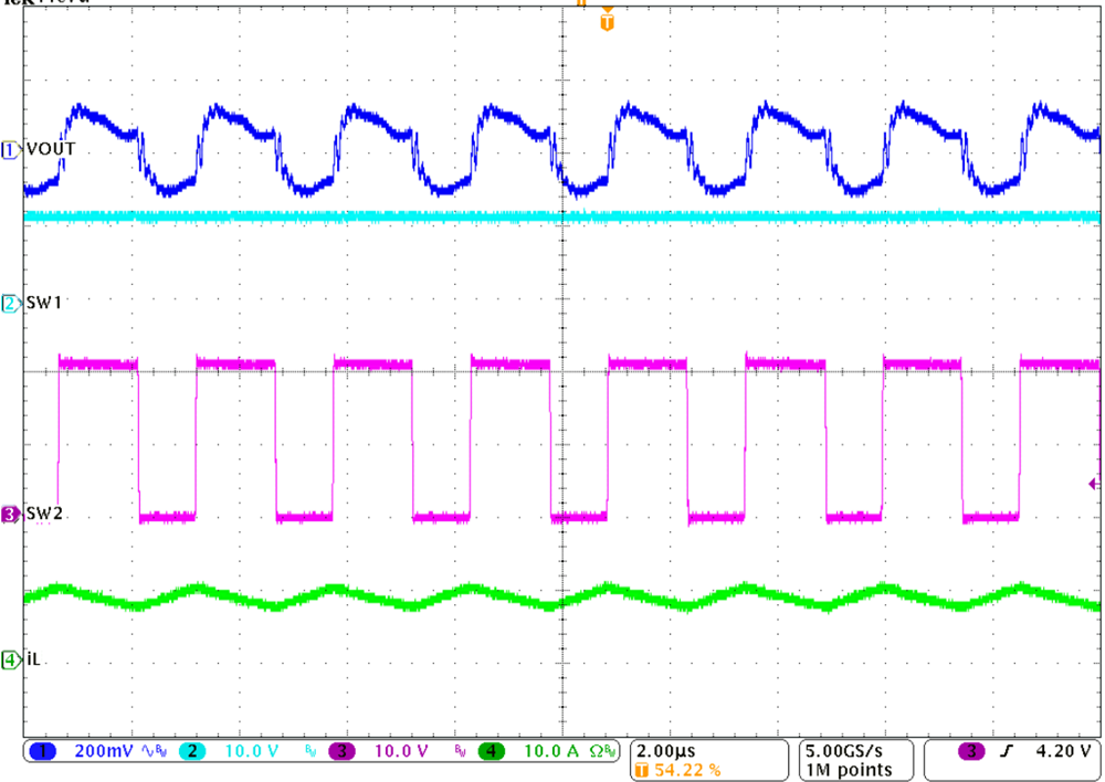 Figure 8-6 Switching Waveforms in
VIN = 12 V, VOUT = 20 V, IO = 5 A,
FPWM
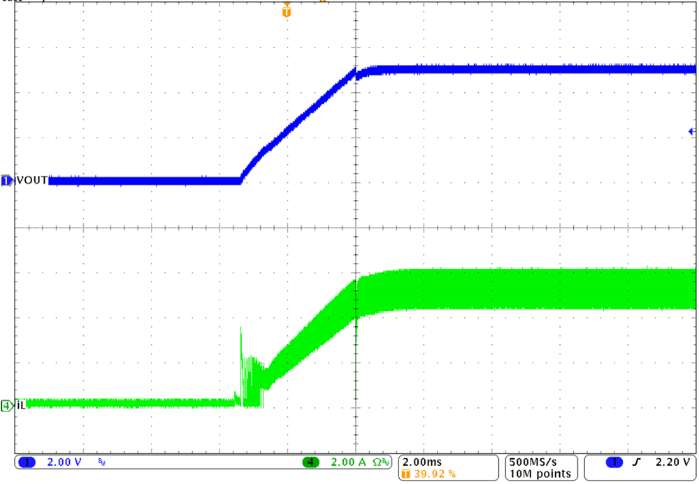 Figure 8-8 Start-up Waveforms in
VIN = 12 V, VOUT = 5 V, IO = 5 A,
FPWM
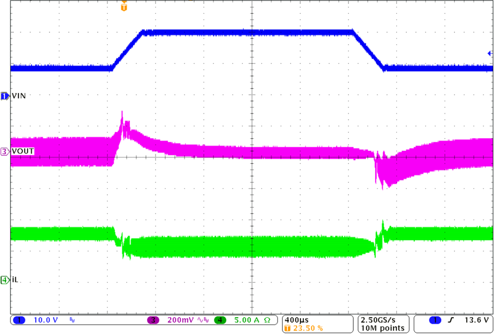 Figure 8-10 Line Transient Waveforms
in VIN = 9 V to 20 V, VOUT = 12 V, IO = 5 A
with 200-μs Slew Rate, FPWM
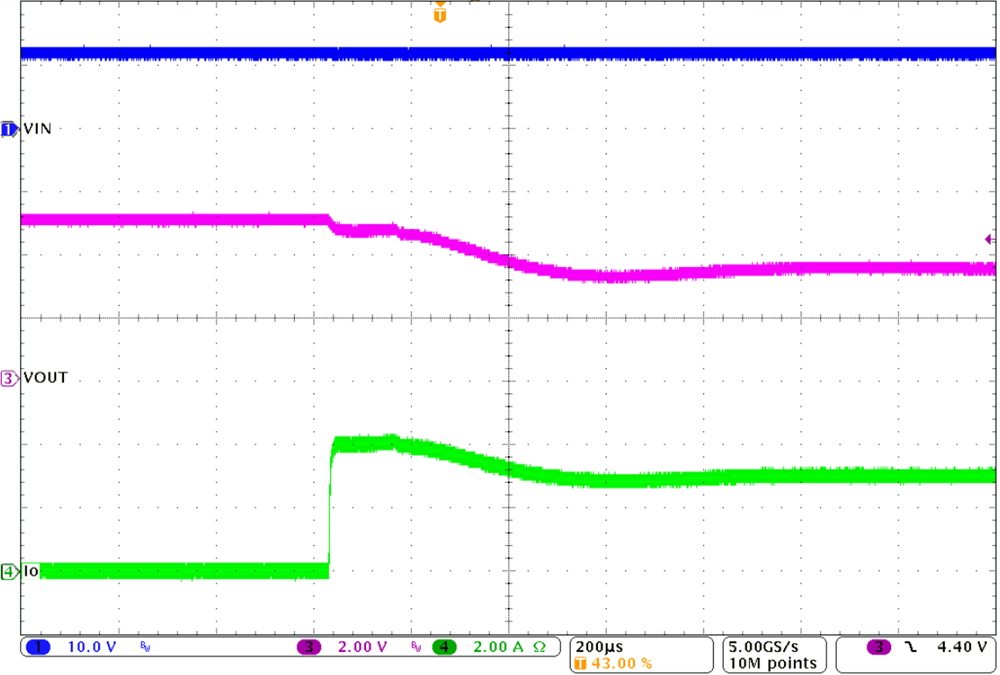 Figure 8-12 3-A Output Current Limit
Waveforms in VIN = 12 V,
Figure 8-12 3-A Output Current Limit
Waveforms in VIN = 12 V,VOUT = 5 V, RLOAD = 1.2 Ω, FPWM
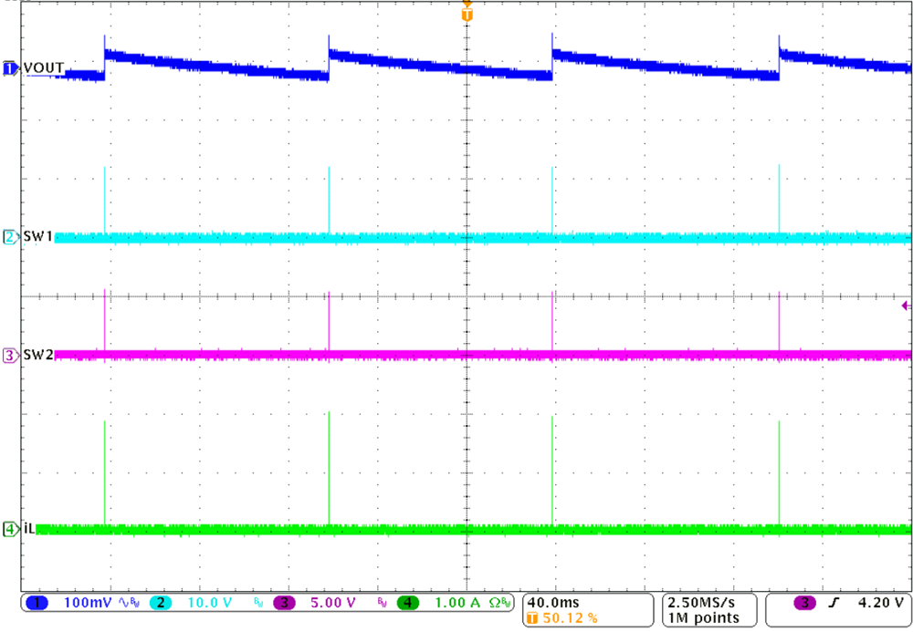 Figure 8-3 Switching Waveforms in VIN = 12 V, VOUT = 5 V,
IO = 0 A, PFM
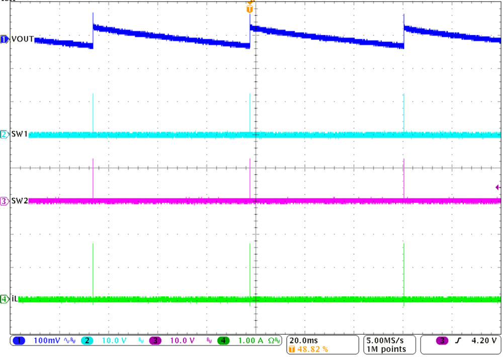 Figure 8-5 Switching Waveforms in
VIN = 12 V, VOUT = 12 V, IO = 0 A,
PFM
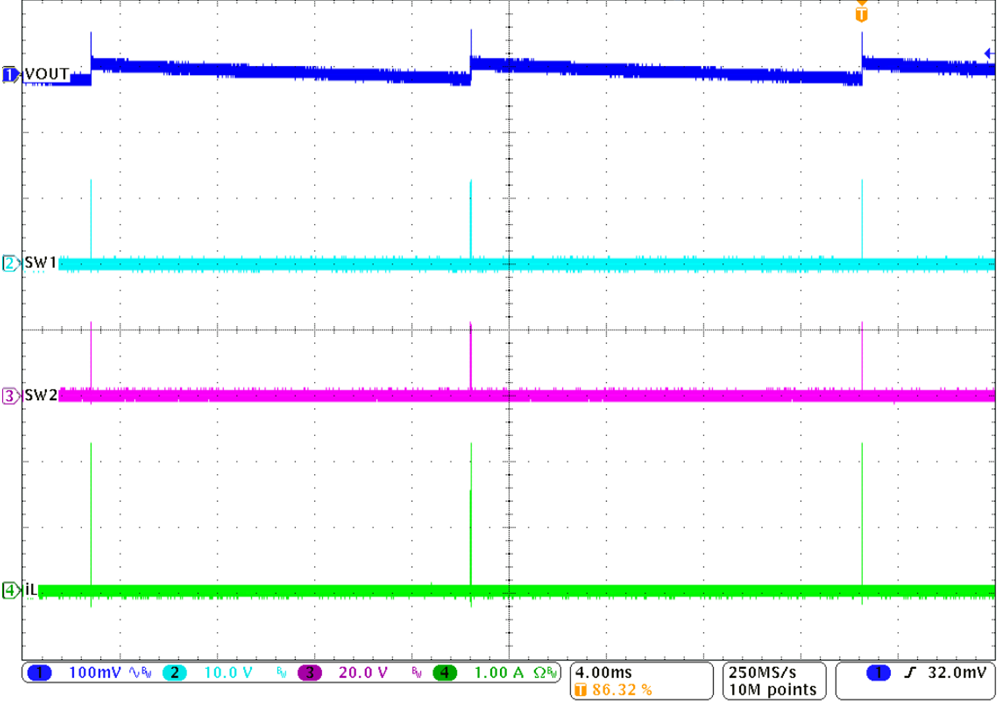 Figure 8-7 Switching Waveforms in
VIN = 12 V, VOUT = 20 V, IO = 0 A,
PFM
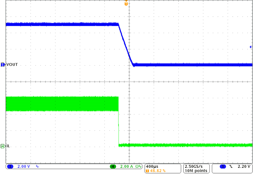 Figure 8-9 Shutdown Waveforms in
VIN = 12 V, VOUT = 5 V, IO = 5 A,
FPWM
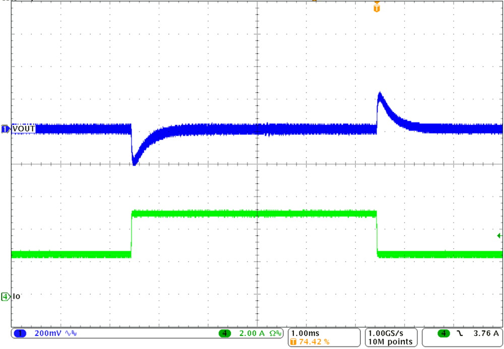 Figure 8-11 Load Transient Waveforms
in VIN = 12 V, VOUT = 5 V, IO = 2.5 A to 5
A with 20-μs Slew Rate, FPWM