SLVSFC5 November 2020 TPS552882
PRODUCTION DATA
- 1 Features
- 2 Applications
- 3 Description
- 4 Revision History
- 5 Pin Configuration and Functions
- 6 Specifications
-
7 Detailed Description
- 7.1 Overview
- 7.2 Functional Block Diagram
- 7.3
Feature Description
- 7.3.1 VCC Power Supply
- 7.3.2 Operation Mode Setting
- 7.3.3 Input Undervoltage Lockout
- 7.3.4 Enable and Programmable UVLO
- 7.3.5 Soft Start
- 7.3.6 Shutdown
- 7.3.7 Switching Frequency
- 7.3.8 Switching Frequency Dithering
- 7.3.9 Inductor Current Limit
- 7.3.10 Internal Charge Path
- 7.3.11 Output Voltage Setting
- 7.3.12 Output Current Indication and Cable Voltage Drop Compensation
- 7.3.13 Integrated Gate Drivers
- 7.3.14 Output Current Limit
- 7.3.15 Overvoltage Protection
- 7.3.16 Output Short Circuit Protection
- 7.3.17 Thermal Shutdown
- 7.4 Device Functional Modes
- 8 Application and Implementation
- 9 Power Supply Recommendations
- 10Layout
- 11Device and Documentation Support
Package Options
Mechanical Data (Package|Pins)
- RPM|26
Thermal pad, mechanical data (Package|Pins)
- RPM|26
Orderable Information
6.6 Typical Characteristics
VIN = 12 V, TA = 25°C, fSW = 400 kHz,
unless otherwise noted.
VIN = 12 V, TA = 25°C, fSW = 400 kHz,
unless otherwise noted.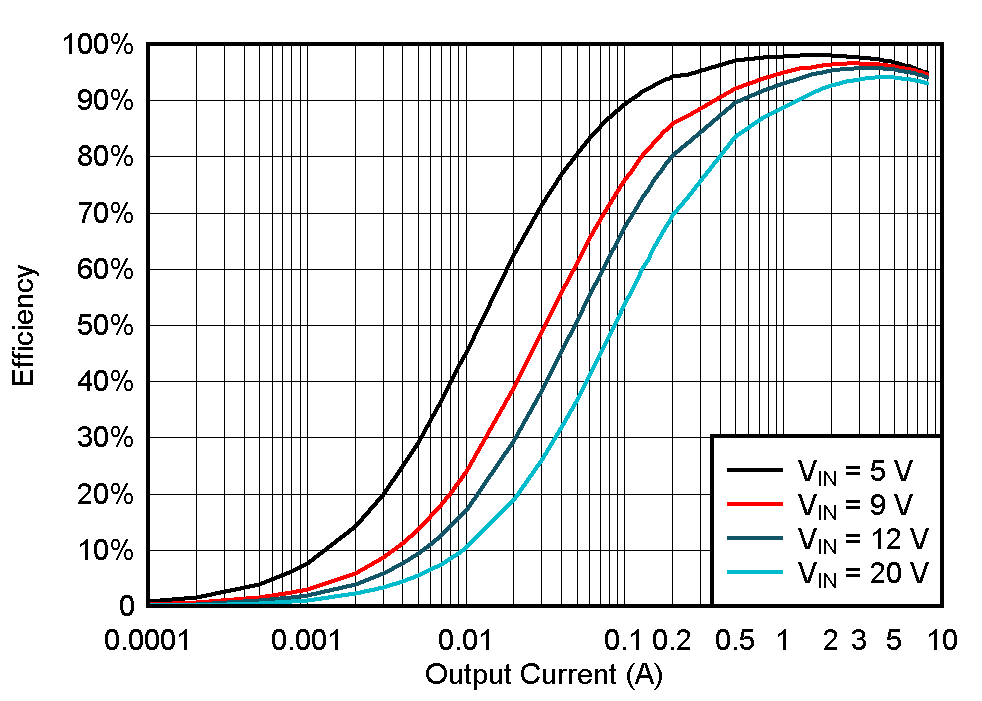 Figure 6-1 Efficiency vs Output Current,
VOUT = 5 V, FPWM. VIN = 12 V, TA = 25°C, fSW = 400 kHz, unless otherwise noted.
 Figure 6-1 Efficiency vs Output Current,
 VOUT = 5 V, FPWM. VIN = 12 V, TA = 25°C, fSW = 400 kHz, unless otherwise noted.
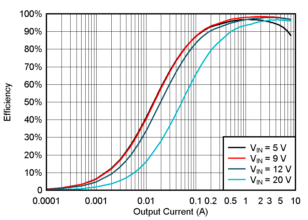 Figure 6-3 Efficiency vs Output
Current,
 VOUT = 9 V, FPWM
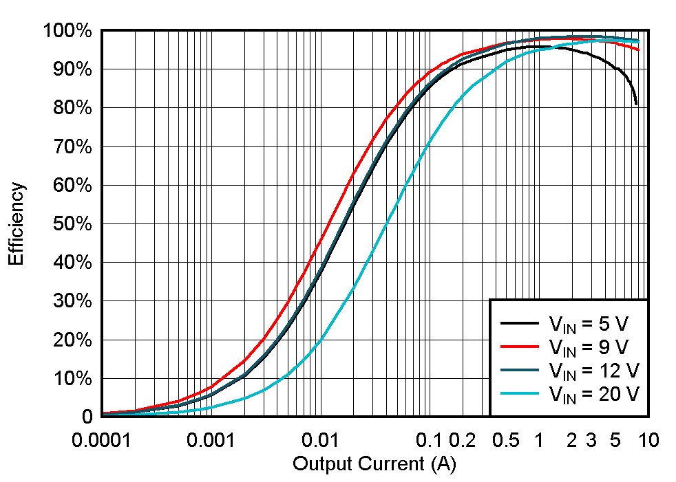 Figure 6-5 Efficiency vs Output
Current,
 VOUT = 12 V, FPWM
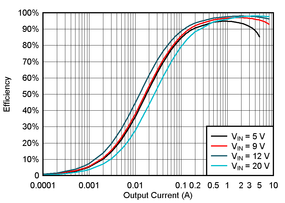 Figure 6-7 Efficiency vs Output
Current,
 VOUT = 15 V, FPWM
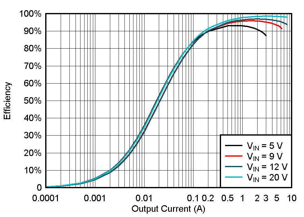 Figure 6-9 Efficiency vs Output
Current,
 VOUT = 20 V, FPWM
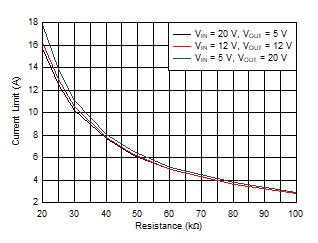 Figure 6-11 Average Inductor Current
Limit vs Setting Resistance
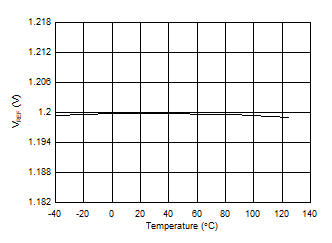 Figure 6-13 Reference Voltage vs
Temperature (VREF = 1.2 V)
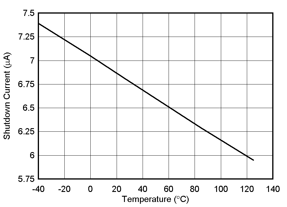 Figure 6-15 Shutdown Current vs
Temperature
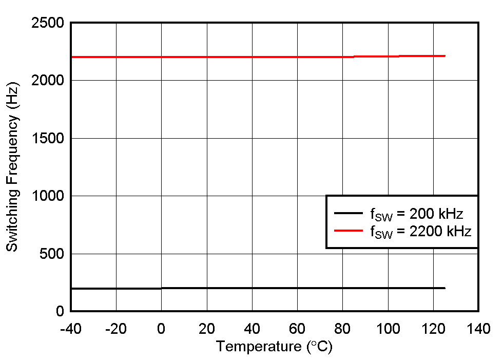 Figure 6-17 Switching Frequency vs
Temperature
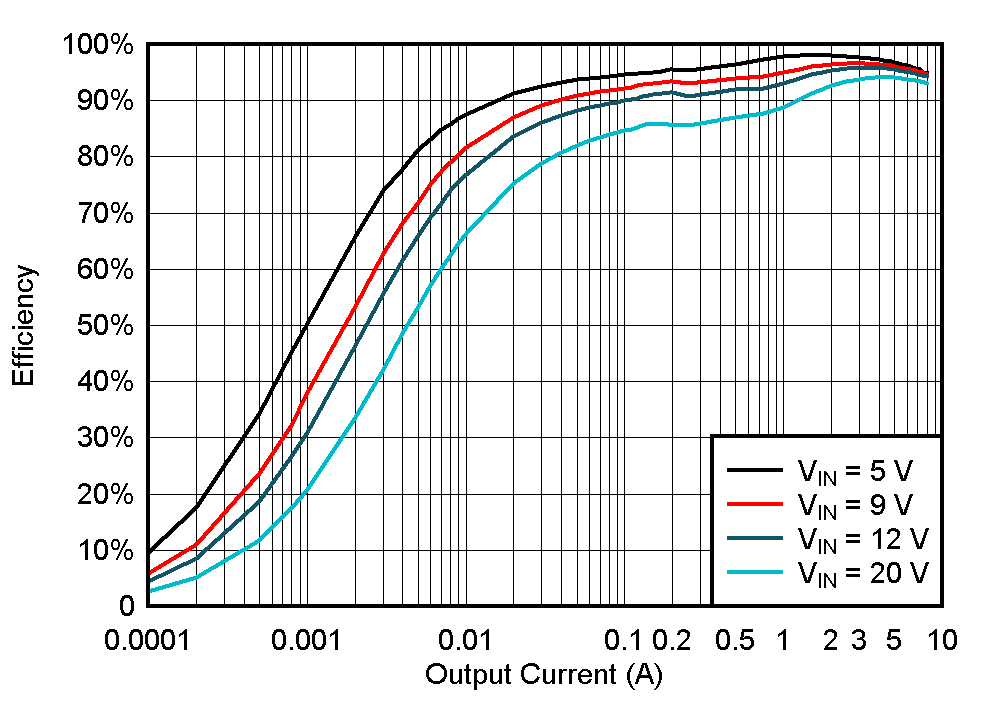 Figure 6-2 Efficiency vs Output Current,
 VOUT = 5 V, PFM
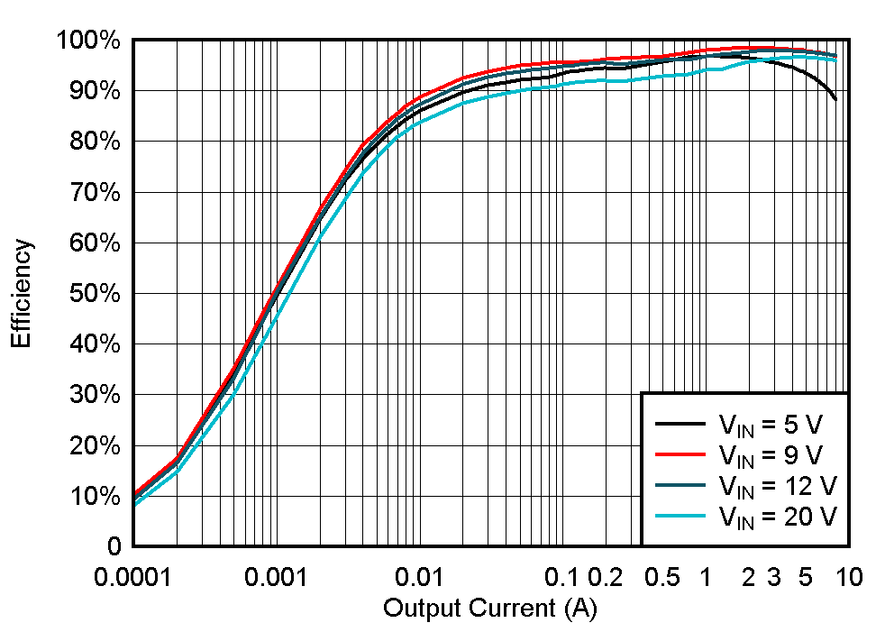 Figure 6-4 Efficiency vs Output
Current,
 VOUT = 9 V, PFM
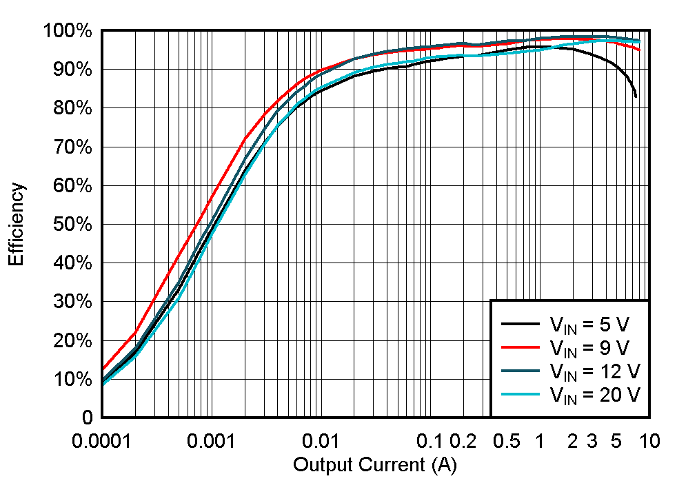 Figure 6-6 Efficiency vs Output
Current,
 VOUT = 12 V, PFM
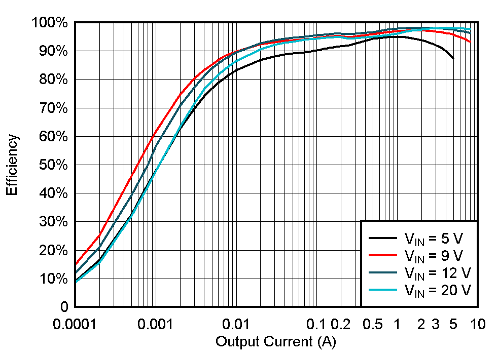 Figure 6-8 Efficiency vs Output
Current,
 VOUT = 15 V, PFM
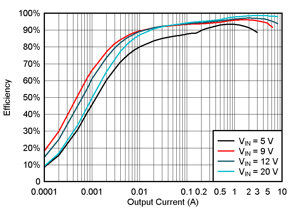 Figure 6-10 Efficiency vs Output
Current,
 VOUT = 20 V, PFM
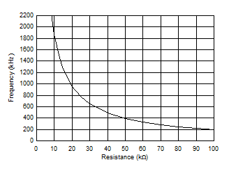 Figure 6-12 Switching Frequency vs
Setting Resistance
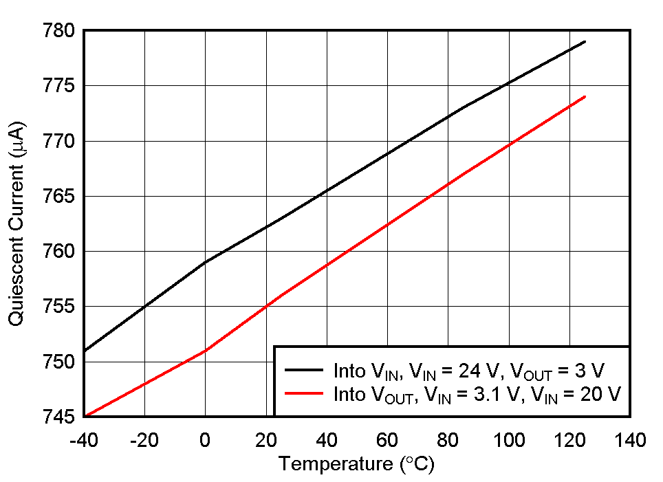 Figure 6-14 Quiescent Current vs
Temperature
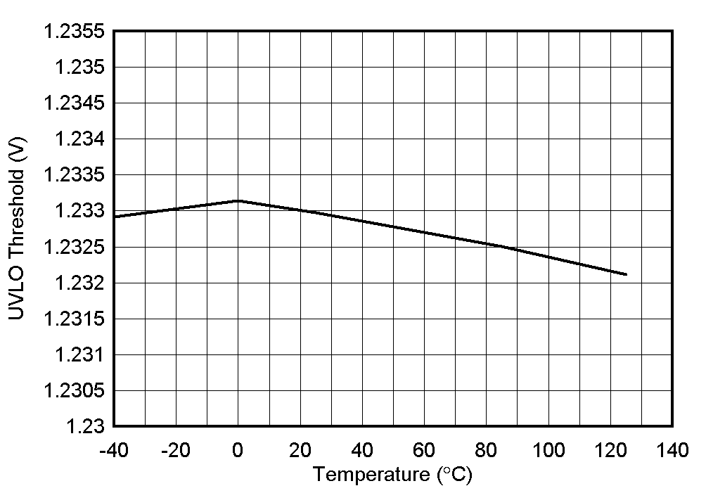 Figure 6-16 ENABLE/UVLO Rising
Threshold vs Temperature
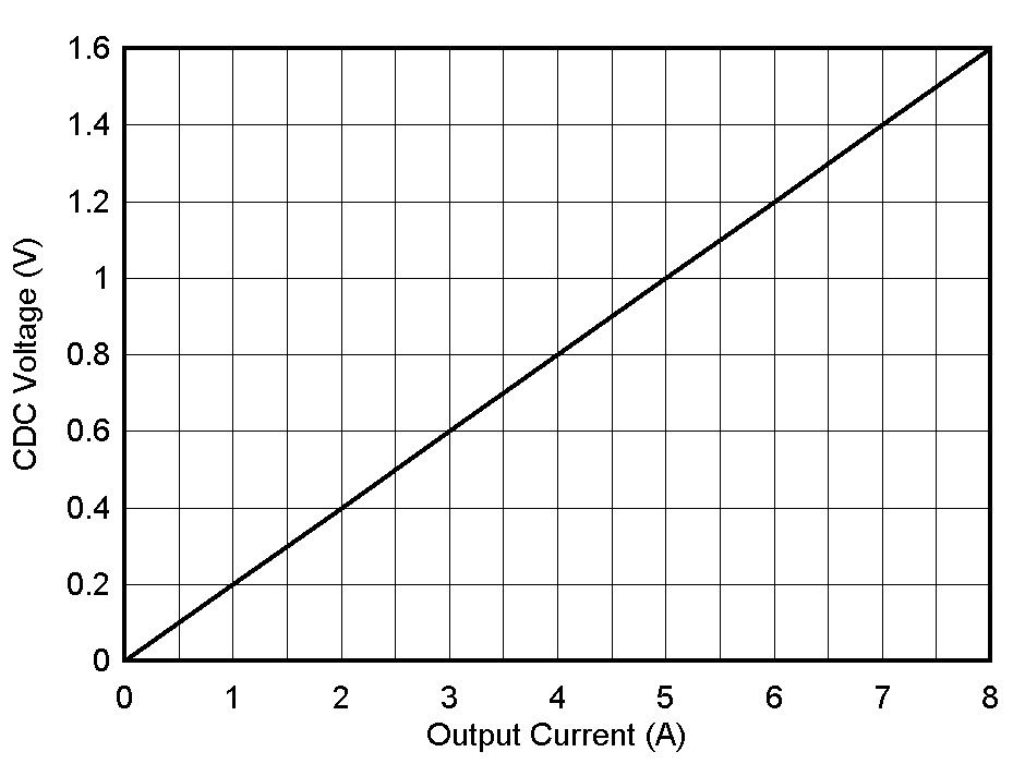 Figure 6-18 CDC Voltage vs Output
Current with RSENSE = 10 mΩ