SLVSC81C September 2013 – February 2016 TPS560200
PRODUCTION DATA.
- 1 Features
- 2 Applications
- 3 Description
- 4 Revision History
- 5 Pin Configuration and Functions
- 6 Specifications
- 7 Detailed Description
- 8 Application and Implementation
- 9 Power Supply Recommendations
- 10Layout
- 11Device and Documentation Support
- 12Mechanical, Packaging, and Orderable Information
Package Options
Mechanical Data (Package|Pins)
- DBV|5
Thermal pad, mechanical data (Package|Pins)
Orderable Information
1 Features
- Integrated Monolithic 0.95-Ω High-Side and 0.33-Ω Low-Side MOSFETs
- 500-mA Continuous Output Current
- Output Voltage Range: 0.8 V to 6.5 V
- 0.8-V Voltage Reference With ±1.3% Accuracy Over Temperature
- Auto-Skip Advanced Eco-Mode™ for High Efficiency at Light Loads
- D-CAP2™ Mode Enables Fast Transient Responses
- No External Compensation Needed
- 600-kHz Switching Frequency
- 2-ms Internal Soft-Start
- Safe Start-Up into Prebiased VOUT
- Thermal Shutdown
- –40°C to 125°C Operating Junction Temperature Range
- Available in 5-Pin SOT-23 Package
2 Applications
- Set Top Boxes
- Modems
- DTBs
- ASDLs
3 Description
The TPS560200 is an 17-V, 500-mA, low-Iq, adaptive on-time D-CAP2 mode synchronous monolithic buck converter with integrated MOSFETs in easy-to-use 5-pin SOT-23 package.
The TPS560200 lets system designers complete the suite of various end-equipment power bus regulators with a cost-effective, low component count and low standby current solution. The main control loop for the device uses the D-CAP2 mode control that provides a fast transient response with no external compensation components. The adaptive on-time control supports seamless transition between PWM mode at higher load conditions and advanced Eco-Mode operation at light loads.
The TPS560200 also has a proprietary circuit that enables the device to adopt to both low equivalent series resistance (ESR) output capacitors, such as POSCAP or SP-CAP, and ultra-low ESR ceramic capacitors. The device operates from 4.5-V to 17-V VIN input. The output voltage can be programmed between 0.8 V and 6.5 V. The device also features a fixed 2-ms soft-start time. The device is available in the 5-pin SOT-23 package.
Device Information(1)
| PART NUMBER | PACKAGE | BODY SIZE (NOM) |
|---|---|---|
| TPS560200 | SOT (5) | 2.90 mm × 1.60 mm |
- For all available packages, see the orderable addendum at the end of the datasheet.
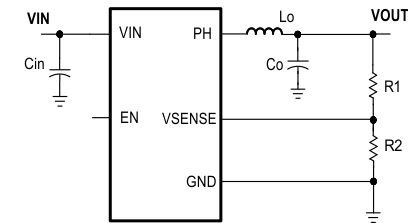
Simplified Schematic
