SLVSD91D December 2015 – September 2024 TPS562201 , TPS562208
PRODUCTION DATA
- 1
- 1 Features
- 2 Applications
- 3 Description
- 4 Pin Configuration and Functions
- 5 Specifications
- 6 Detailed Description
- 7 Application and Implementation
- 8 Device and Documentation Support
- 9 Revision History
- 10Mechanical, Packaging, and Orderable Information
Package Options
Refer to the PDF data sheet for device specific package drawings
Mechanical Data (Package|Pins)
- DDC|6
Thermal pad, mechanical data (Package|Pins)
Orderable Information
10.1 Tape and Reel Information
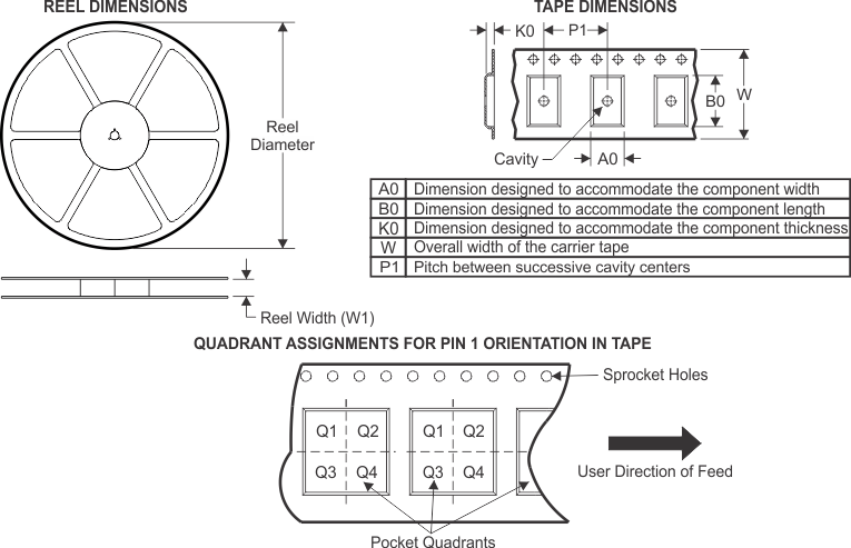
| Device | Package Type |
Package Drawing | Pins | SPQ | Reel Diameter (mm) |
Reel Width W1 (mm) |
A0 (mm) |
B0 (mm) |
K0 (mm) |
P1 (mm) |
W (mm) |
Pin1 Quadrant |
|---|---|---|---|---|---|---|---|---|---|---|---|---|
| TPS562201DDCR | SOT-23- THIN | DDC | 6 | 3000 | 180.0 | 8.4 | 3.2 | 3.2 | 1.4 | 4.0 | 8.0 | Q3 |
| TPS562208DDCR | SOT-23- THIN | DDC | 6 | 3000 | 180.0 | 8.4 | 3.2 | 3.2 | 1.4 | 4.0 | 8.0 | Q3 |
| TPS562208DDCR | SOT-23- THIN | DDC | 6 | 3000 | 180.0 | 8.4 | 3.2 | 3.2 | 1.4 | 4.0 | 8.0 | Q3 |
| TPS562208DDCT | SOT-23- THIN | DDC | 6 | 250 | 180.0 | 8.4 | 3.2 | 3.2 | 1.4 | 4.0 | 8.0 | Q3 |
| TPS562208DDCT | SOT-23- THIN | DDC | 6 | 250 | 180.0 | 8.4 | 3.2 | 3.2 | 1.4 | 4.0 | 8.0 | Q3 |
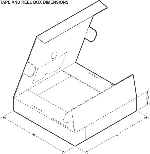
| Device | Package Type | Package Drawing | Pins | SPQ | Length (mm) | Width (mm) | Height (mm) |
|---|---|---|---|---|---|---|---|
| TPS562201DDCR | SOT-23-THIN | DDC | 6 | 3000 | 210.0 | 185.0 | 35.0 |
| TPS562208DDCR | SOT-23-THIN | DDC | 6 | 3000 | 210.0 | 185.0 | 35.0 |
| TPS562208DDCR | SOT-23-THIN | DDC | 6 | 3000 | 210.0 | 185.0 | 35.0 |
| TPS562208DDCT | SOT-23-THIN | DDC | 6 | 250 | 210.0 | 185.0 | 35.0 |
| TPS562208DDCT | SOT-23-THIN | DDC | 6 | 250 | 210.0 | 185.0 | 35.0 |


