SLUSED6 October 2020 TPS562202S
PRODUCTION DATA
- 1 Features
- 2 Applications
- 3 Description
- 4 Revision History
- 5 Device Comparison Table
- 6 Pin Configuration and Functions
- 7 Specifications
- 8 Detailed Description
- 9 Application and Implementation
- 10Power Supply Recommendations
- 11Layout
- 12Device and Documentation Support
- 13Mechanical, Packaging, and Orderable Information
Package Options
Mechanical Data (Package|Pins)
- DRL|6
Thermal pad, mechanical data (Package|Pins)
Orderable Information
9.2.3 Application Curves
Below waveforms are tested at VIN = 12 V, unless otherwise noted.
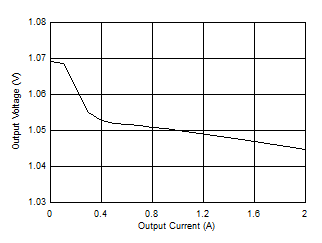
 Figure 9-2 Load Regulation with
Different Loading
 Figure 9-4 Input Voltage Ripple
Iout = 2 A
 Figure 9-6 Output Voltage Ripple,
Iout = 0.2 A
 Figure 9-8 Start-up Relative to
VIN
 Figure 9-10 Start-up Relative to
EN
 Figure 9-12 Transient Response, 0.2 to
1.8 A
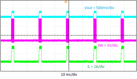
 Figure 9-14 OC
 Figure 9-3 Load Regulation with
Different Input Voltage
 Figure 9-5 Output Voltage Ripple,
Iout = 0.01 A
 Figure 9-7 Output Voltage Ripple,
Iout = 2 A
 Figure 9-9 Shutdown Relative to
VIN
 Figure 9-11 Shutdown Relative to
EN
 Figure 9-13 Transient Response, 1 to 2
A
 Figure 9-15 Hiccup, Iout = 5 A