SLUSED6 October   2020 TPS562202S

PRODUCTION DATA  

  1. Features
  2. Applications
  3. Description
  4. Revision History
  5. Device Comparison Table
  6. Pin Configuration and Functions
  7. Specifications
    1. 7.1 Absolute Maximum Ratings
    2. 7.2 ESD Ratings
    3. 7.3 Recommended Operating Conditions
    4. 7.4 Thermal Information
    5. 7.5 Electrical Characteristics
    6. 7.6 Typical Characteristics
  8. Detailed Description
    1. 8.1 Overview
    2. 8.2 Functional Block Diagram
    3. 8.3 Feature Description
      1. 8.3.1 Adaptive On-Time Control and PWM Operation
      2. 8.3.2 ECO Mode Control
      3. 8.3.3 Soft Start and Pre-Biased Soft Start
      4. 8.3.4 Current Protection
      5. 8.3.5 Undervoltage Lockout (UVLO) Protection
      6. 8.3.6 Thermal Shutdown
    4. 8.4 Device Functional Modes
      1. 8.4.1 Normal Operation
      2. 8.4.2 Eco-mode Operation
  9. Application and Implementation
    1. 9.1 Application Information
    2. 9.2 Typical Application
      1. 9.2.1 Design Requirements
      2. 9.2.2 Detailed Design Procedure
        1. 9.2.2.1 Output Voltage Resistors Selection
        2. 9.2.2.2 Output Filter Selection
        3. 9.2.2.3 Input Capacitor Selection
        4. 9.2.2.4 Bootstrap Capacitor Selection
      3. 9.2.3 Application Curves
  10. 10Power Supply Recommendations
  11. 11Layout
    1. 11.1 Layout Guidelines
    2. 11.2 Layout Example
  12. 12Device and Documentation Support
    1. 12.1 Receiving Notification of Documentation Updates
    2. 12.2 Support Resources
    3. 12.3 Trademarks
    4. 12.4 Electrostatic Discharge Caution
    5. 12.5 Glossary
  13. 13Mechanical, Packaging, and Orderable Information

Package Options

Mechanical Data (Package|Pins)
Thermal pad, mechanical data (Package|Pins)
Orderable Information

Typical Application

The application schematic in Figure 9-1 was developed to meet the previous requirements. This circuit is available as the evaluation module (EVM). The following sections provide the design procedure.

Figure 9-1 shows the TPS562202S 4.3-V to 17-V input, 1.05-V output converter schematics.
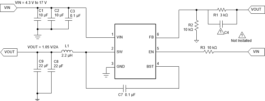
GUID-3B2D507E-A33D-4379-84AD-1A207B565E23-low.gifFigure 9-1 1.05-V/2-A Reference Design