SLUSED6 October 2020 TPS562202S
PRODUCTION DATA
- 1 Features
- 2 Applications
- 3 Description
- 4 Revision History
- 5 Device Comparison Table
- 6 Pin Configuration and Functions
- 7 Specifications
- 8 Detailed Description
- 9 Application and Implementation
- 10Power Supply Recommendations
- 11Layout
- 12Device and Documentation Support
- 13Mechanical, Packaging, and Orderable Information
Package Options
Mechanical Data (Package|Pins)
- DRL|6
Thermal pad, mechanical data (Package|Pins)
Orderable Information
6 Pin Configuration and Functions
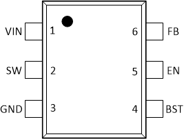
 Figure 6-1 6-Pin SOT563 DRL Package (Top
View)
Figure 6-1 6-Pin SOT563 DRL Package (Top
View)Table 6-1 Pin Functions
| PIN | I/O | DESCRIPTION | |
|---|---|---|---|
| NAME | NO. | ||
| VIN | 1 | I | Input voltage supply pin |
| SW | 2 | O | Switch node connection between high-side NFET and low-side NFET |
| GND | 3 | — | Ground pin source terminal of low-side power NFET as well as the ground terminal for controller circuit. Connect sensitive FB to this GND at a single point. |
| BST | 4 | O | Supply input for the high-side NFET gate drive circuit. Connect 0.1-μF capacitor between BST and SW pin. |
| EN | 5 | I | Enable input control. Active high. Must be pulled up to enable the device. |
| FB | 6 | I | Converter feedback input. Connect to output voltage with feedback resistor divider. |