SLUSAH5D MARCH 2011 – February 2016 TPS56221
PRODUCTION DATA.
- 1 Features
- 2 Applications
- 3 Description
- 4 Revision History
- 5 Pin Configuration and Functions
- 6 Specifications
-
7 Detailed Description
- 7.1 Overview
- 7.2 Functional Block Diagram
- 7.3 Feature Description
- 7.4 Device Functional Modes
-
8 Application and Implementation
- 8.1 Application Information
- 8.2
Typical Application
- 8.2.1 Design Requirements
- 8.2.2
Detailed Design Procedure
- 8.2.2.1 Switching Frequency Selection
- 8.2.2.2 Inductor Selection
- 8.2.2.3 Output Capacitor Selection
- 8.2.2.4 Inductor Peak Current Rating
- 8.2.2.5 Input Capacitor Selection
- 8.2.2.6 Boot-Strap Capacitor (C14)
- 8.2.2.7 Boot-Strap Resistor (R2)
- 8.2.2.8 VDD Bypass Capacitor (C11)
- 8.2.2.9 BP5 Bypass Capacitor (C12)
- 8.2.2.10 Soft-Start Capacitor (C13)
- 8.2.2.11 Current Limit (R1)
- 8.2.2.12 Feedback Divider (R4, R7)
- 8.2.2.13 Compensation (C15, C16, C17, R3, R6)
- 8.2.3 Application Curves
- 9 Power Supply Recommendations
- 10Layout
- 11Device and Documentation Support
- 12Mechanical, Packaging, and Orderable Information
Package Options
Refer to the PDF data sheet for device specific package drawings
Mechanical Data (Package|Pins)
- DQP|22
Thermal pad, mechanical data (Package|Pins)
- DQP|22
Orderable Information
8 Application and Implementation
NOTE
Information in the following applications sections is not part of the TI component specification, and TI does not warrant its accuracy or completeness. TI’s customers are responsible for determining suitability of components for their purposes. Customers should validate and test their design implementation to confirm system functionality.
8.1 Application Information
The TPS56221 is highly integrated synchronous step-down DC-DC converters. The device is used to convert a higher DC input voltage (4.5 V to 14 V recommended) to a lower DC output voltage (as low as 0.6 V), with a maximum output current of 25 A, for a variety of applications. Use the following design procedure to select key component values for this device.
8.2 Typical Application
This design example describes a 25-A, 12-V to 1.0-V design using the TPS56221 high-current integrated buck converter. The system specifications are listed in Table 1.
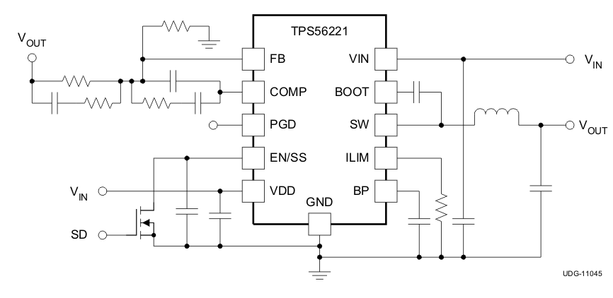 Figure 20. Typical Application Schematic
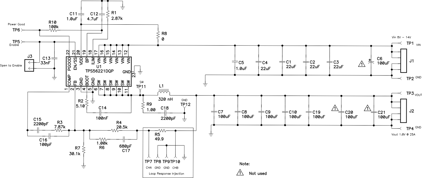 Figure 21. Design Example Schematic
8.2.1 Design Requirements
Table 1. Design Example Parameters
| PARAMETER | TEST CONDITIONS | MIN | TYP | MAX | UNIT | |
|---|---|---|---|---|---|---|
| VIN | Input voltage | 8.0 | 14 | V | ||
| VIN(ripple) | Input ripple | IOUT = 25 A | 0.2 | V | ||
| VOUT | Output voltage | 0 A ≤ IOUT ≤ 25 A | 0.98 | 1.00 | 1.02 | V |
| Line regulation | 8 V ≤ VIN ≤ 14 V | 0.1% | ||||
| Load regulation | 0 A ≤ IOUT ≤ 25 A | 1.0% | ||||
| VP-P | Output ripple | IOUT= 25 A | 20 | mV | ||
| VOVER | Output overshoot | ITRAN = 10 A | 100 | mV | ||
| VUNDER | Output undershoot | ITRAN = 10 A | 100 | mV | ||
| IOUT | Output current | 8 V ≤ VIN ≤ 14 V | 0 | 25 | A | |
| tSS | Softstart time | VIN = 12 V | 2.0 | ms | ||
| ISCP | Short circuit current trip point | 32 | A | |||
| η | Efficiency | VIN = 12 V, IOUT = 25 A | 87% | |||
| fSW | Switching frequency | 500 | kHz | |||
8.2.2 Detailed Design Procedure
Table 2. List of Materials for TPS56221 Design Example
| REFERENCE DESiGNATOR |
QTY | VALUE | DESCRIPTION | SIZE | PART NUMBER | MANUFACTURER |
|---|---|---|---|---|---|---|
| C1, C2, C3, C4 | 4 | 22 µF | Capacitor, Ceramic, 25 V, X5R, 20% | 1210 | Std | Std |
| C5, C11 | 2 | 1.0 µF | Capacitor, Ceramic, 25 V, X7R, 20% | 0805 | Std | Std |
| C6 | 0 | 100 µF | Capacitor, Ceramic, 16 Vdc, ±20% | Code D8 | Std | EEEFP1C101AP |
| C7, C8, C9, C10, C19 | 5 | 100 µF | Capacitor, Ceramic, 6.3 V, X5R, 20% | 1210 | Std | Std |
| C12 | 1 | 4.7 µF | Capacitor, Ceramic, 10 V, X5R, 20% | 0805 | Std | Std |
| C13 | 1 | 33 nF | Capacitor, Ceramic, 16 V, X7R, 20% | 0603 | Std | Std |
| C14 | 1 | 100 nF | Capacitor, Ceramic, 16V, X7R, 20% | 0402 | Std | Std |
| C15, C18 | 2 | 2200 pF | Capacitor, Ceramic, 50 V, X7R, 10% | 0603 | Std | Std |
| C16 | 1 | 100 pF | Capacitor, Ceramic, 50 V, C0G, 10% | 0603 | Std | Std |
| C17 | 1 | 680 pF | Capacitor, Ceramic, 50 V, C0G, 10% | 0603 | Std | Std |
| C20, C21 | 0 | 100 µF | Capacitor, Ceramic, 6.3 V, X5R, 20% | 1210 | Std | Std |
| J1, J2 | 2 | Terminal Block, 4-pin, 15-A, 5.1 mm | 0.80 x 0.35 inch | ED120/4DS | ||
| J3 | 1 | Header, Male 2-pin, 100 mil spacing | 0.100 inch x 2 | PEC02SAAN | ||
| L1 | 1 | 320 nH | Inductor, 320 nH, 41 A, 0.32 mΩ | 0.530 x 0.510 inch | PA2202-321NL | Pulse |
| R1 | 1 | 1.78 kΩ | Resistor, Chip, 1/16W, 1% | 0603 | Std | Std |
| R2 | 1 | 5.10 Ω | Resistor, Chip, 1/16W, 1% | 0603 | Std | Std |
| R3 | 1 | 7.87 kΩ | Resistor, Chip, 1/16W, 1% | 0603 | Std | Std |
| R4 | 1 | 20.5 kΩ | Resistor, Chip, 1/16W, 1% | 0603 | Std | Std |
| R5 | 49.9Ω | Resistor, Chip, 1/16W, 1% | 0603 | |||
| R6 | 1 | 1.00 kΩ | Resistor, Chip, 1/16W, 1% | 0603 | Std | Std |
| R7 | 1 | 30.1 kΩ | Resistor, Chip, 1/16W, 1% | 0603 | Std | Std |
| R8 | 1 | 0 Ω | Resistor, Chip, 1/16W, 1% | 0603 | ||
| R9 | 1 | 1 Ω | Resistor, Chip, 1/16W, 1% | 0603 | ||
| R10 | 1 | 100 kΩ | Resistor, Chip, 1/16W, 1% | 0603 | ||
| TP1, TP3, TP11 | 3 | Test Point, Red, Thru Hole | 0.125 x 0.125 inch | 5010 | ||
| TP2, TP4, TP8, TP9, TP12 | 5 | Test Point, Black, Thru Hole | 0.125 x 0.125 inch | 5011 | ||
| TP5, TP6 | 2 | Test Point, Yellow, Thru Hole | 0.125 x 0.125 inch | 5014 | ||
| TP7, TP10 | 2 | Test Point, White, Thru Hole | 0.125 x 0.125 inch | 5012 | ||
| U1 | 1 | QFN-22 | 4.5-V to 14-V Input, 25-A, synchronous buck converter | 6 × 5 mm | TPS56221DQP | TI |
8.2.2.1 Switching Frequency Selection
To achieve a balance between small size and high efficiency for this design, use switching frequency of 500 kHz.
8.2.2.2 Inductor Selection
Synchronous buck power inductors are typically sized for between approximately 20% and 40% peak-to-peak ripple current (IP-P).
Using this target ripple current, the required inductor size can be calculated as shown in Equation 3.

Selecting a standard 320-nH inductor value, IP-P = 5.8 A.
The RMS current through the inductor is approximated in Equation 4.

8.2.2.3 Output Capacitor Selection
The selection of the output capacitor is typically driven by the output transient response. For applications with VIN(min) > 2 x VOUT, use overshoot to calculate the minimum output capacitance and the equation is shown in Equation 5.

For applications where VIN(min) < 2 × VOUT, use undershoot to calculate minimum output capacitance. The equation is shown in Equation 6.

To meet the low ESR and high-capacitance requirements of this design, five 100-µF, 1210 ceramic capacitors are selected. With a minimum capacitance, the maximum allowable ESR is determined by the maximum ripple voltage and is approximated by Equation 7.

8.2.2.4 Inductor Peak Current Rating
With output capacitance, it is possible to calculate the charge current during start-up and determine the minimum saturation current rating for the inductor. The start-up charging current is approximated by Equation 8.

The peak current in the inductor IL(peak) is approximated by Equation 9.

With the short circuit current trip point IOUT(max) set at 32 A, the maximum allowable peak current IL(peak max) is

The selection of output capacitor meets the maximum allowable peak current requirement.
Table 3. Inductor Requirements Summary
| PARAMETER | VALUE | UNIT | |
|---|---|---|---|
| L | Inductance | 320 | nH |
| IL(rms) | RMS current (thermal rating) | 25.1 | A |
| IL(peak max) | Peak current (saturation rating) | 32.9 | A |
The PA0513.321NLT, 320-nH, 0.32-mΩ, 41-A inductor is selected.
8.2.2.5 Input Capacitor Selection
The input voltage ripple is divided between capacitance and ESR. For this design VIN_RIPPLE(CAP) = 150 mV and VIN_RIPPLE(ESR) = 50 mV. The minimum capacitance and maximum ESR are estimated in Equation 11.


The RMS current in the input capacitors is estimated by Equation 13.

Four 1210, 22-µF, 25-V, X5R ceramic capacitors with about 2.5-mΩ of ESR and a 2.5-A RMS current rating are selected. Higher voltage capacitors are selected to minimize capacitance loss at the DC bias voltage to ensure the capacitors will have sufficient capacitance at the working voltage while a 1.0-µF capacitor in smaller case size is used to reduce high frequency noise from the MOSFET switching.
8.2.2.6 Boot-Strap Capacitor (C14)
The bootstrap capacitor maintains power to the high-side driver during the high-side switch ON time. Per the requirements of the integrated MOSFET, CBOOT is 100 nF with a minimum 10-V rating.
8.2.2.7 Boot-Strap Resistor (R2)
The bootstrap resistor slows the rising edge of the SW voltage to reduce ringing and improve EMI. Per the datasheet recommendation a 5.10-Ω resistor is selected.
8.2.2.7.1 RC Snubber (R9 and C18)
To effectively limit the switch node ringing, a 1.0-Ω resistor and a 2200-pF capacitor are selected.
8.2.2.8 VDD Bypass Capacitor (C11)
In accordance with pin terminations recommended in the data sheet, VDD is bypassed to GND with a 1.0-µF capacitor.
8.2.2.9 BP5 Bypass Capacitor (C12)
Per the datasheet recommended pin terminations, BP5 is bypassed to GND with at least 1.0-µF capacitor. For additional filtering and noise immunity a 4.7-µF capacitor is selected.
8.2.2.10 Soft-Start Capacitor (C13)
The soft-start capacitor provides a constant ramp voltage to the error amplifier to provide controlled, smooth start-up. The soft-start capacitor is sized using Equation 14.

8.2.2.11 Current Limit (R1)
The TPS56221 uses the negative drop across the internal low-side FET at the end of the OFF-time to measure the valley of the inductor current. Allowing for a minimum of 30% over maximum load, the programming resistor is selected using Equation 15.

A standard 2.87-kΩ resistor is selected from the E-48 series.
8.2.2.12 Feedback Divider (R4, R7)
The TPS56221 converter uses a full operational amplifier with an internally fixed 0.600-V reference. R4 is selected between 10 kΩ and 50 kΩ for a balance of feedback current and noise immunity. With R4 set to 20.5 kΩ, The output voltage is programmed with a resistor divider given by Equation 16.

A standard 30.1-kΩ resistor is selected from the E-48 series.
8.2.2.13 Compensation (C15, C16, C17, R3, R6)
Using the TPS40k Loop Stability Tool for 50 kHz of bandwidth and 60 degrees of phase margin with an R4 value of 20.5 kΩ, the following values are obtained.
- C17 = C_1 = 680 pF
- C15 = C_2 = 2200 pF
- C16 = C_3 = 100 pF
- R6 = R_2 = 1.00 kΩ
- R3 = R_3 = 7.87 kΩ
8.2.3 Application Curves
Output voltage 12 V to 1.0 V, input current 0 A to 25 A.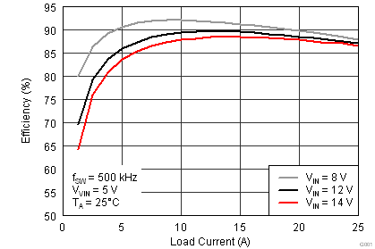 Figure 22. Efficiency vs Load Current
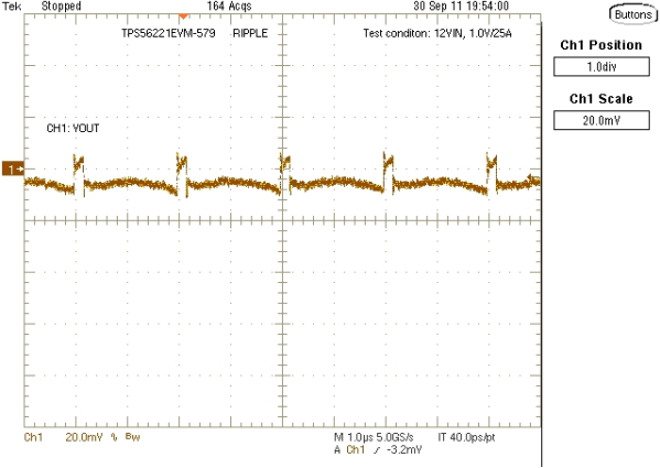 Figure 24. TPS56221 Design Example Output Ripple 20 mV/div, 1.0 µs/div, 20 MHz Bandwidth, AC Coupled
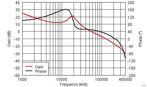 Figure 23. Loop Response 51 kHz Bandwidth, 48° Phase Margin