SLUSDA4B February   2019  – October 2019 TPS562231

PRODUCTION DATA.  

  1. Features
  2. Applications
  3. Description
    1.     Device Images
      1.      Simplified Schematic
      2.      TPS562231 Efficiency
  4. Revision History
  5. Pin Configuration and Functions
    1.     Pin Functions
  6. Specifications
    1. 6.1 Absolute Maximum Ratings
    2. 6.2 ESD Ratings
    3. 6.3 Recommended Operating Conditions
    4. 6.4 Thermal Information
    5. 6.5 Electrical Characteristics
    6. 6.6 Typical Characteristics
  7. Detailed Description
    1. 7.1 Overview
    2. 7.2 Functional Block Diagram
    3. 7.3 Feature Description
      1. 7.3.1 Adaptive On-Time Control and PWM Operation
      2. 7.3.2 Soft Start and Pre-Biased Soft Start
      3. 7.3.3 Over Current and Short Circuit Protection
      4. 7.3.4 Undervoltage Lockout (UVLO) Protection
      5. 7.3.5 Thermal Shutdown
    4. 7.4 Device Functional Modes
      1. 7.4.1 Shutdown Mode
      2. 7.4.2 Continuous Conduction Mode (CCM)
      3. 7.4.3 Pulse Skip Mode (PSM, TPS562231)
  8. Application and Implementation
    1. 8.1 Application Information
    2. 8.2 Typical Application
      1. 8.2.1 Design Requirements
      2. 8.2.2 Detailed Design Procedure
        1. 8.2.2.1 Output Voltage Resistors Selection
        2. 8.2.2.2 Output Filter Selection
        3. 8.2.2.3 Input Capacitor Selection
        4. 8.2.2.4 Bootstrap Capacitor Selection
      3. 8.2.3 Application Curves
  9. Power Supply Recommendations
  10. 10Layout
    1. 10.1 Layout Guidelines
    2. 10.2 Layout Example
  11. 11Device and Documentation Support
    1. 11.1 Device Support
    2. 11.2 Receiving Notification of Documentation Updates
    3. 11.3 Community Resources
    4. 11.4 Trademarks
    5. 11.5 Electrostatic Discharge Caution
    6. 11.6 Glossary
  12. 12Mechanical, Packaging, and Orderable Information

Package Options

Mechanical Data (Package|Pins)
Thermal pad, mechanical data (Package|Pins)
Orderable Information

Typical Application

The TPS562231 only require a few external components to convert from a higher variable voltage supply to a fixed output voltage. Figure 13 shows a basic schematic of 3.3-V output application. This section provides the design procedure.
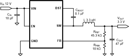
TPS562231 app-cir-SLUSD65.gifFigure 13. TPS562231 3.3V/2-A Reference Design