SLUSDA4B February   2019  – October 2019 TPS562231

PRODUCTION DATA.  

  1. Features
  2. Applications
  3. Description
    1.     Device Images
      1.      Simplified Schematic
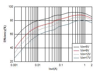
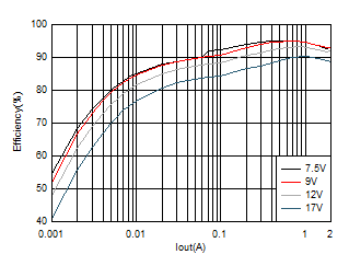
      2.      TPS562231 Efficiency
  4. Revision History
  5. Pin Configuration and Functions
    1.     Pin Functions
  6. Specifications
    1. 6.1 Absolute Maximum Ratings
    2. 6.2 ESD Ratings
    3. 6.3 Recommended Operating Conditions
    4. 6.4 Thermal Information
    5. 6.5 Electrical Characteristics
    6. 6.6 Typical Characteristics
  7. Detailed Description
    1. 7.1 Overview
    2. 7.2 Functional Block Diagram
    3. 7.3 Feature Description
      1. 7.3.1 Adaptive On-Time Control and PWM Operation
      2. 7.3.2 Soft Start and Pre-Biased Soft Start
      3. 7.3.3 Over Current and Short Circuit Protection
      4. 7.3.4 Undervoltage Lockout (UVLO) Protection
      5. 7.3.5 Thermal Shutdown
    4. 7.4 Device Functional Modes
      1. 7.4.1 Shutdown Mode
      2. 7.4.2 Continuous Conduction Mode (CCM)
      3. 7.4.3 Pulse Skip Mode (PSM, TPS562231)
  8. Application and Implementation
    1. 8.1 Application Information
    2. 8.2 Typical Application
      1. 8.2.1 Design Requirements
      2. 8.2.2 Detailed Design Procedure
        1. 8.2.2.1 Output Voltage Resistors Selection
        2. 8.2.2.2 Output Filter Selection
        3. 8.2.2.3 Input Capacitor Selection
        4. 8.2.2.4 Bootstrap Capacitor Selection
      3. 8.2.3 Application Curves
  9. Power Supply Recommendations
  10. 10Layout
    1. 10.1 Layout Guidelines
    2. 10.2 Layout Example
  11. 11Device and Documentation Support
    1. 11.1 Device Support
    2. 11.2 Receiving Notification of Documentation Updates
    3. 11.3 Community Resources
    4. 11.4 Trademarks
    5. 11.5 Electrostatic Discharge Caution
    6. 11.6 Glossary
  12. 12Mechanical, Packaging, and Orderable Information

Package Options

Mechanical Data (Package|Pins)
Thermal pad, mechanical data (Package|Pins)
Orderable Information

Typical Characteristics

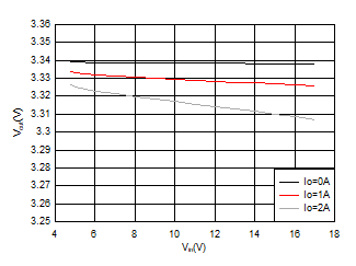
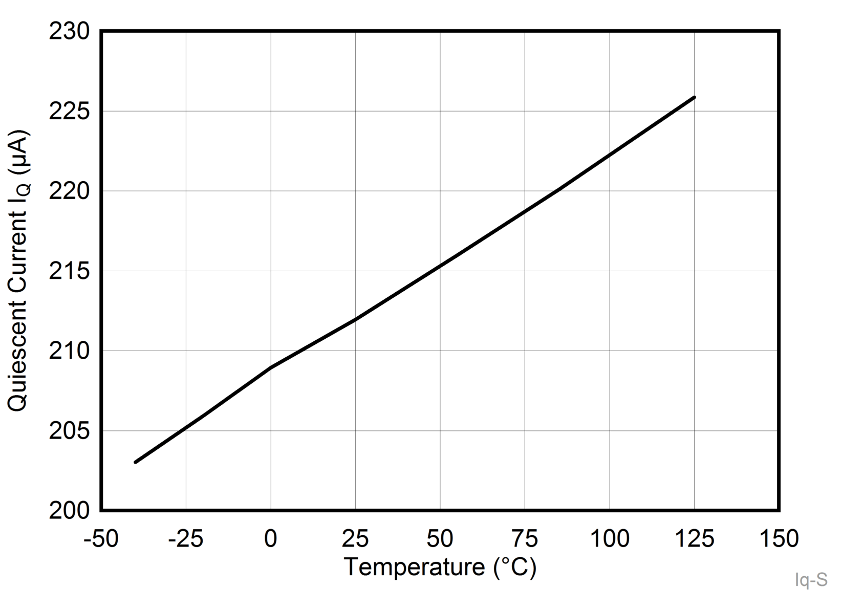
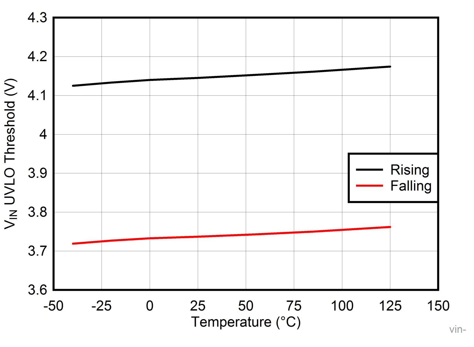
VIN = 12 V (unless otherwise noted)
TPS562231 Iq-SLUSD65.gif
Figure 1. IQ vs Junction Temperature
TPS562231 vin-uvlo-SLUSD65.gif
Figure 3. VIN UVLO vs Junction Temperature
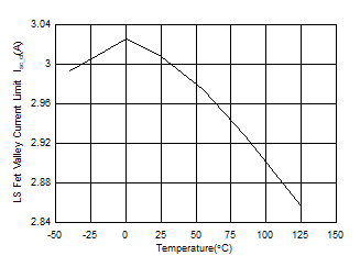
TPS562231 ValleyCurrentLimit_1P1_SLUDSA4.gif
Figure 5. Current Limit vs Junction Temperature
TPS562231 TPS562231_1V05_Efficiency_1P1.gif
Figure 7. TPS562231 VOUT = 1.05 V Efficiency
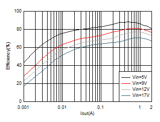
TPS562231 TPS562231_3V3_Efficiency_1P1.gif
Figure 9. TPS562231 VOUT = 3.3 V Efficiency
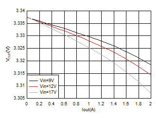
TPS562231 TPS562231_3V3_LoadRegulation.gif
Figure 11. TPS562231 VOUT = 3.3V Load Regulation
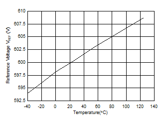
TPS562231 ReferenceVoltage_1P1_SLUDA4.gif
Figure 2. VREF Voltage vs Junction Temperature
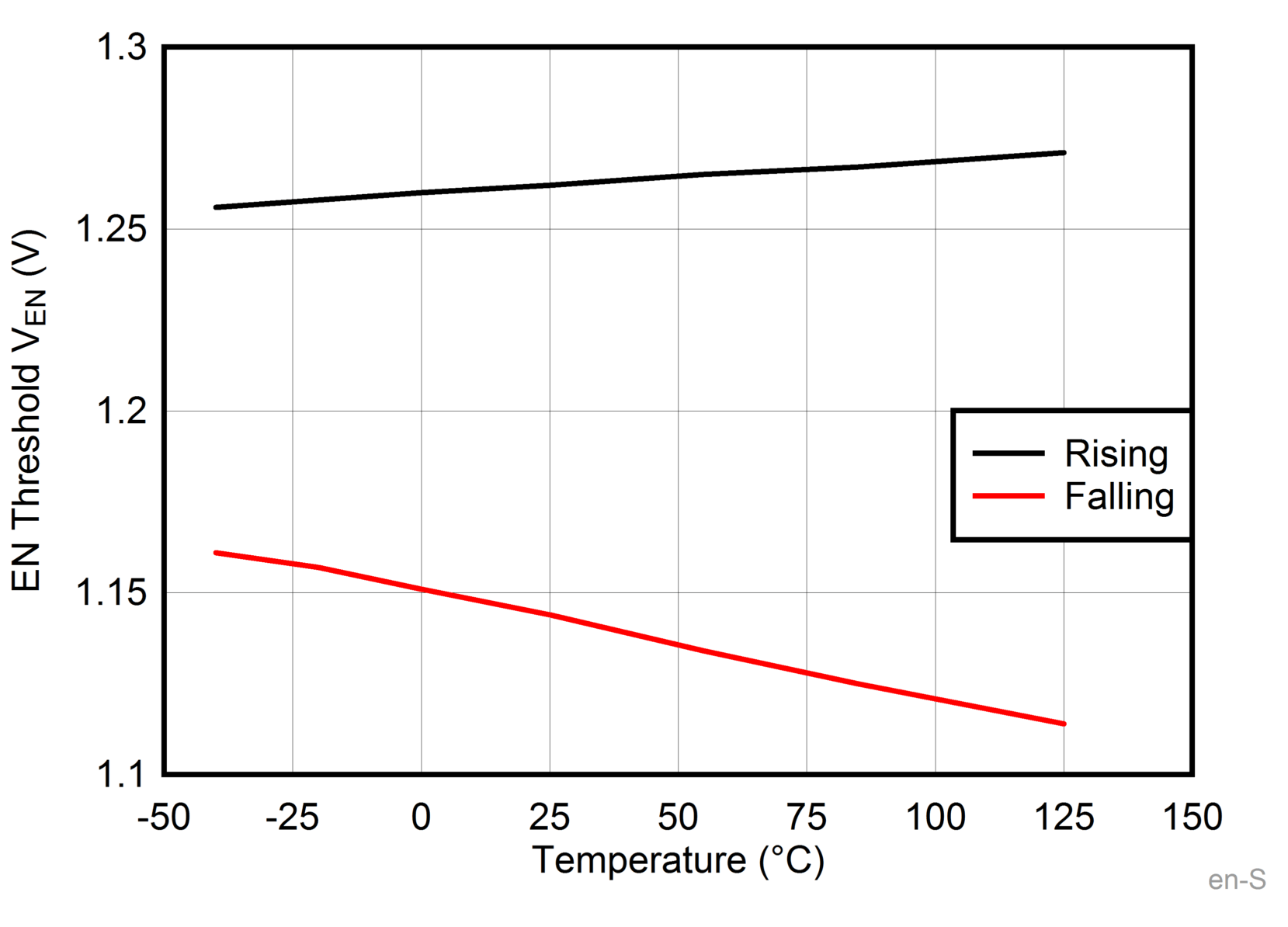
TPS562231 en-SLUSD65.gif
Figure 4. EN Pin UVLO vs Junction Temperature
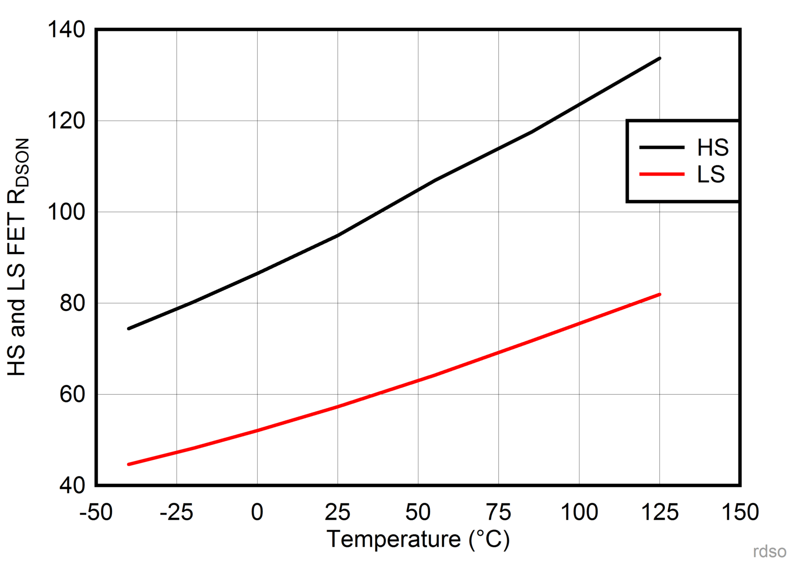
TPS562231 rdson-SLUSD65.gif
Figure 6. RDS-ON vs Junction Temperature
TPS562231 TPS562231_1V8_Efficiency_1P1.gif
Figure 8. TPS562231 VOUT = 1.8 V Efficiency
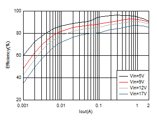
TPS562231 TPS562231_5V_Efficiency_1P1.gif
Figure 10. TPS562231 VOUT = 5 V Efficiency
TPS562231 TPS562231_3V3_LineRegulation.gif
Figure 12. TPS562231 VOUT = 3.3 V Line Regulation