SLUSDX1A September 2020 – August 2021 TPS563211
PRODUCTION DATA
- 1 Features
- 2 Applications
- 3 Description
- 4 Revision History
- 5 Pin Configuration and Functions
- 6 Specifications
-
7 Detailed Description
- 7.1 Overview
- 7.2 Functional Block Diagram
- 7.3
Feature Description
- 7.3.1 Advanced Emulated Current Mode Control
- 7.3.2 Mode Selection and PG/SS Pin Function Configuration
- 7.3.3 Power Good (PG)
- 7.3.4 Soft Start and Pre-Biased Soft Start
- 7.3.5 Output Discharge through PG/SS Pin
- 7.3.6 Precise Enable and Adjusting Undervoltage Lockout
- 7.3.7 Overcurrent Limit and Undervoltage Protection
- 7.3.8 Overvoltage Protection
- 7.3.9 Thermal Shutdown
- 7.4 Device Functional Modes
- 8 Application and Implementation
- 9 Power Supply Recommendations
- 10Layout
- 11Device and Documentation Support
- 12Mechanical, Packaging, and Orderable Information
Package Options
Mechanical Data (Package|Pins)
- DRL|8
Thermal pad, mechanical data (Package|Pins)
Orderable Information
7.3.5 Output Discharge through PG/SS Pin
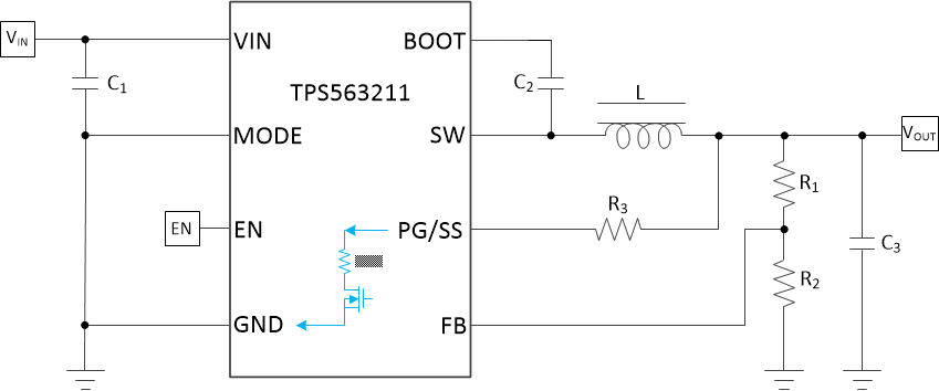
If the PG function is selected, the device pulls the PG/SS pin low when the device is shut down by EN, OVP, UVP, UVLO, or thermal shutdown. Connecting PG/SS to VOUT through a resistor can be used to discharge VOUT in those cases (see Figure 7-2). The discharge rate can be adjusted by R3, which is also used to pull up the PG/SS pin in normal operation. The minimum supply voltage required for the discharge function to remain active is typically 2.5 V. For reliability, keep the maximum current into the PG/SS pin less than 1.8 mA. Given an output voltage, the minimum resistance of R3 can be calculated in Equation 11.

 Figure 7-2 Discharge
VOUT through PG/SS Pin with TPS563211