SLUSES9 July 2022 TPS563300
PRODUCTION DATA
- 1 Features
- 2 Applications
- 3 Description
- 4 Revision History
- 5 Pin Configuration and Functions
- 6 Specifications
-
7 Detailed Description
- 7.1 Overview
- 7.2 Functional Block Diagram
- 7.3
Feature Description
- 7.3.1 Fixed Frequency Peak Current Mode
- 7.3.2 Pulse Frequency Modulation
- 7.3.3 Voltage Reference
- 7.3.4 Output Voltage Setting
- 7.3.5 Enable and Adjusting Undervoltage Lockout
- 7.3.6 Minimum On Time, Minimum Off Time, and Frequency Foldback
- 7.3.7 Frequency Spread Spectrum
- 7.3.8 Overvoltage Protection
- 7.3.9 Overcurrent and Undervoltage Protection
- 7.3.10 Thermal Shutdown
- 7.4 Device Functional Modes
-
8 Application and Implementation
- 8.1 Application Information
- 8.2
Typical Application
- 8.2.1 Design Requirements
- 8.2.2
Detailed Design Procedure
- 8.2.2.1 Custom Design With WEBENCH® Tools
- 8.2.2.2 Output Voltage Resistors Selection
- 8.2.2.3 Bootstrap Capacitor Selection
- 8.2.2.4 Undervoltage Lockout Set Point
- 8.2.2.5 Output Inductor Selection
- 8.2.2.6 Output Capacitor Selection
- 8.2.2.7 Input Capacitor Selection
- 8.2.2.8 Feedforward Capacitor CFF Selection
- 8.2.2.9 Maximum Ambient Temperature
- 8.2.3 Application Curves
- 8.3 Best Design Practices
- 8.4 Power Supply Recommendations
- 8.5 Layout
- 9 Device and Documentation Support
- 10Mechanical, Packaging, and Orderable Information
Package Options
Mechanical Data (Package|Pins)
- DRL|8
Thermal pad, mechanical data (Package|Pins)
Orderable Information
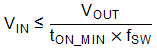
7.4.5 Minimum On-Time Operation
Every switching converter has a minimum controllable on time dictated by the inherent delays and blanking times associated with the control circuits, which imposes a minimum switch duty cycle and, therefore, a minimum conversion ratio. The constraint is encountered at high input voltages and low output voltages. To help extend the minimum controllable duty cycle, the TPS563300 automatically reduces the switching frequency when the minimum on-time limit is reached. This way, the converter can regulate the lowest programmable output voltage at the maximum input voltage. Use Equation 11 to find an estimate for the approximate input voltage for a given output voltage before frequency foldback occurs. The values of tON_MIN and fSW can be found in Section 6.5.
As the input voltage is increased, the switch on time (duty-cycle) reduces to regulate the output voltage. When the on time reaches the minimum on time, tON_MIN, the switching frequency drops while the on time remains fixed.