SLVSDJ7B May 2016 – August 2017 TPS564201
PRODUCTION DATA.
- 1 Features
- 2 Applications
- 3 Description
- 4 Revision History
- 5 Pin Configuration and Functions
- 6 Specifications
- 7 Detailed Description
- 8 Application and Implementation
- 9 Power Supply Recommendations
- 10Layout
- 11Device and Documentation Support
- 12Mechanical, Packaging, and Orderable Information
Package Options
Mechanical Data (Package|Pins)
- DDC|6
Thermal pad, mechanical data (Package|Pins)
Orderable Information
8 Application and Implementation
NOTE
Information in the following applications sections is not part of the TI component specification, and TI does not warrant its accuracy or completeness. TI’s customers are responsible for determining suitability of components for their purposes. Customers should validate and test their design implementation to confirm system functionality.
8.1 Application Information
The device is a typical step-down DC-DC converter for converting a higher dc voltage to a lower dc voltage with a maximum available output current of 4 A. The following design procedure can be used to select component values for the TPS564201. Alternately, the WEBENCH® software may be used to generate a complete design. The WEBENCH software uses an iterative design procedure and accesses a comprehensive database of components when generating a design. This section presents a simplified discussion of the design process.
8.2 Typical Application
The application schematic in Figure 14 shows the TPS564201 4.5-V to 17-V input, 1.05-V output converter design meeting the requirements for 4-A output. This circuit is available as the evaluation module (EVM). The sections provide the design procedure.
8.2.1 Design Requirements
Table 1 shows the design parameters for this application.
Table 1. Design Parameters
| PARAMETER | EXAMPLE VALUE |
|---|---|
| Input voltage range | 4.5 to 17 V |
| Output voltage | 1.05 V |
| Transient response, 2-A load step | ΔVout = ±5% |
| Input ripple voltage | 400 mV |
| Output ripple voltage | 30 mV |
| Output current rating | 4 A |
| Operating frequency | 560 kHz |
8.2.2 Detailed Design Procedure
8.2.2.1 Custom Design With WEBENCH® Tools
Click here to create a custom design using the TPS564201 device with the WEBENCH® Power Designer.
- Start by entering the input voltage (VIN), output voltage (VOUT), and output current (IOUT) requirements.
- Optimize the design for key parameters such as efficiency, footprint, and cost using the optimizer dial.
- Compare the generated design with other possible solutions from Texas Instruments.
The WEBENCH Power Designer provides a customized schematic along with a list of materials with real-time pricing and component availability.
In most cases, these actions are available:
- Run electrical simulations to see important waveforms and circuit performance
- Run thermal simulations to understand board thermal performance
- Export customized schematic and layout into popular CAD formats
- Print PDF reports for the design, and share the design with colleagues
Get more information about WEBENCH tools at www.ti.com/WEBENCH.
8.2.2.2 Output Voltage Resistors Selection
The output voltage is set with a resistor divider from the output node to the VFB pin. TI recommends to use 1% tolerance or better divider resistors. Start by using to calculate VOUT.
To improve efficiency at very light loads consider using larger value resistors. However, using too high of resistance causes the circuit to be more susceptible to noise; and, voltage errors from the VFB input current will be more noticeable.
8.2.2.3 Output Filter Selection
The LC filter used as the output filter has double pole at:

At low frequencies, the overall loop gain is set by the output set-point resistor divider network and the internal gain of the device. The low frequency phase is 180°. At the output filter pole frequency, the gain rolls off at a –40 dB per decade rate and the phase drops rapidly. D-CAP2 introduces a high frequency zero that reduces the gain roll off to –20 dB per decade and increases the phase to 90° one decade above the zero frequency. The inductor and capacitor for the output filter must be selected so that the double pole of Equation 3 is located below the high frequency zero but close enough that the phase boost provided be the high frequency zero provides adequate phase margin for a stable circuit. To meet this requirement use the values recommended in Table 2.
Table 2. Recommended Component Values
| OUTPUT VOLTAGE (V) | R1 (kΩ) | R2 (kΩ) | L1 (µH) | C8 + C9 (µF) | ||
|---|---|---|---|---|---|---|
| MIN | TYP | MAX | ||||
| 1 | 3.09 | 10.0 | 1.5 | 2.2 | 4.7 | 20 to 68 |
| 1.05 | 3.74 | 10.0 | 1.5 | 2.2 | 4.7 | 20 to 68 |
| 1.2 | 5.76 | 10.0 | 1.5 | 2.2 | 4.7 | 20 to 68 |
| 1.5 | 9.53 | 10.0 | 1.5 | 2.2 | 4.7 | 20 to 68 |
| 1.8 | 13.7 | 10.0 | 1.5 | 2.2 | 4.7 | 20 to 68 |
| 2.5 | 22.6 | 10.0 | 2.2 | 2.2 | 4.7 | 20 to 68 |
| 3.3 | 33.2 | 10.0 | 2.2 | 2.2 | 4.7 | 20 to 68 |
| 5 | 54.9 | 10.0 | 3.3 | 3.3 | 4.7 | 20 to 68 |
| 6.5 | 75 | 10.0 | 3.3 | 3.3 | 4.7 | 20 to 68 |
The inductor peak-to-peak ripple current, peak current and RMS current are calculated using Equation 4, Equation 5, and Equation 6. The inductor saturation current rating must be greater than the calculated peak current and the RMS or heating current rating must be greater than the calculated RMS current.
Use 560 kHz for ƒSW. Make sure the chosen inductor is rated for the peak current of Equation 5 and the RMS current of Equation 7.


For this design example, the calculated peak current is 4.4 A and the calculated RMS current is 4 A. The inductor used is a WE 74431122 with a peak current rating of 13 A and an RMS current rating of 9 A.
The capacitor value and ESR determines the amount of output voltage ripple. The TPS564201 is intended for use with ceramic or other low ESR capacitors. Recommended values range from 20 µF to 68 µF. Use Equation 7 to determine the required RMS current rating for the output capacitor.

For this design two TDK C3216X5R0J226M 22-µF output capacitors are used. The typical ESR is 2 mΩ each. The calculated RMS current is 0.286 A and each output capacitor is rated for 4 A.
8.2.2.4 Input Capacitor Selection
The TPS564201 requires an input decoupling capacitor and a bulk capacitor is needed depending on the application. TI recommends a ceramic capacitor over 10 µF for the decoupling capacitor. An additional 0.1-µF capacitor (C3) from pin 3 to ground is optional to provide additional high frequency filtering. The capacitor voltage rating needs to be greater than the maximum input voltage.
8.2.2.5 Bootstrap Capacitor Selection
A 0.1-µF ceramic capacitor must be connected between the VBST to SW pin for proper operation. TI recommends to use a ceramic capacitor.
8.2.3 Application Curves

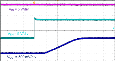
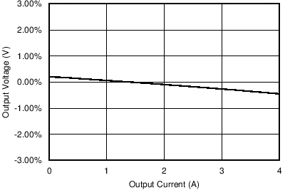
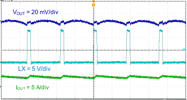
| VIN = 5 V | VOUT = 1.05 V |


| 1 µs/div | ||

| 1 µs/div | ||

| 100 µs/div | ||

| 100 µs/div | ||

| 400 µs/div | ||


| VIN = 12 V | VOUT = 1.05 V |

| VOUT = 1.05 V |

| 1 µs/div | ||

| 1 µs/div | ||

| 100 µs/div | ||

| 2 ms/div | ||

