SLVSE72B September   2017  – June 2018 TPS565208

PRODUCTION DATA.  

  1. Features
  2. Applications
  3. Description
    1.     Device Images
      1.      Simplified Schematic
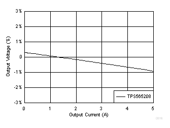
      2.      TPS565208 Load Regulation
  4. Revision History
  5. Pin Configuration and Functions
    1.     Pin Functions
  6. Specifications
    1. 6.1 Absolute Maximum Ratings
    2. 6.2 ESD Ratings
    3. 6.3 Recommended Operating Conditions
    4. 6.4 Thermal Information
    5. 6.5 Electrical Characteristics
    6. 6.6 Typical Characteristics
  7. Detailed Description
    1. 7.1 Overview
    2. 7.2 Functional Block Diagram
    3. 7.3 Feature Description
      1. 7.3.1 Adaptive On-Time Control and PWM Operation
      2. 7.3.2 Soft Start and Pre-Biased Soft Start
      3. 7.3.3 Current Protection
      4. 7.3.4 Undervoltage Lockout (UVLO) Protection
      5. 7.3.5 Thermal Shutdown
    4. 7.4 Device Functional Modes
      1. 7.4.1 Normal Operation
      2. 7.4.2 Standby Operation
  8. Application and Implementation
    1. 8.1 Application Information
    2. 8.2 Typical Application
      1. 8.2.1 Design Requirements
      2. 8.2.2 Detailed Design Procedure
        1. 8.2.2.1 Custom Design With WEBENCH® Tools
        2. 8.2.2.2 Output Voltage Resistors Selection
        3. 8.2.2.3 Output Filter Selection
        4. 8.2.2.4 Input Capacitor Selection
        5. 8.2.2.5 Bootstrap Capacitor Selection
      3. 8.2.3 Application Curves
  9. Power Supply Recommendations
  10. 10Layout
    1. 10.1 Layout Guidelines
    2. 10.2 Layout Example
  11. 11Device and Documentation Support
    1. 11.1 Development Support
      1. 11.1.1 Custom Design With WEBENCH® Tools
    2. 11.2 Receiving Notification of Documentation Updates
    3. 11.3 Community Resources
    4. 11.4 Trademarks
    5. 11.5 Electrostatic Discharge Caution
    6. 11.6 Glossary
  12. 12Mechanical, Packaging, and Orderable Information
    1. 12.1 Package Option Addendum
      1. 12.1.1 Packaging Information
      2. 12.1.2 Tape and Reel Information

Package Options

Mechanical Data (Package|Pins)
Thermal pad, mechanical data (Package|Pins)
Orderable Information

Application Curves

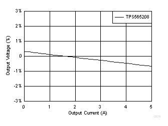
TPS565208 D015_SLVSE72.gif
VIN = 5 V VOUT1 = 1.05 V
Figure 15. TPS565208 Load Regulation, VIN = 5 V
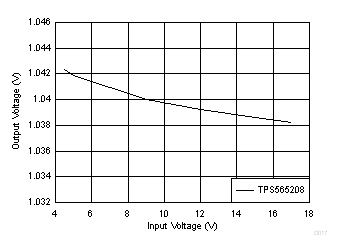
TPS565208 D017_SLVSE72.gif
IOUT = 1 A
Figure 17. TPS565208 Line Regulation
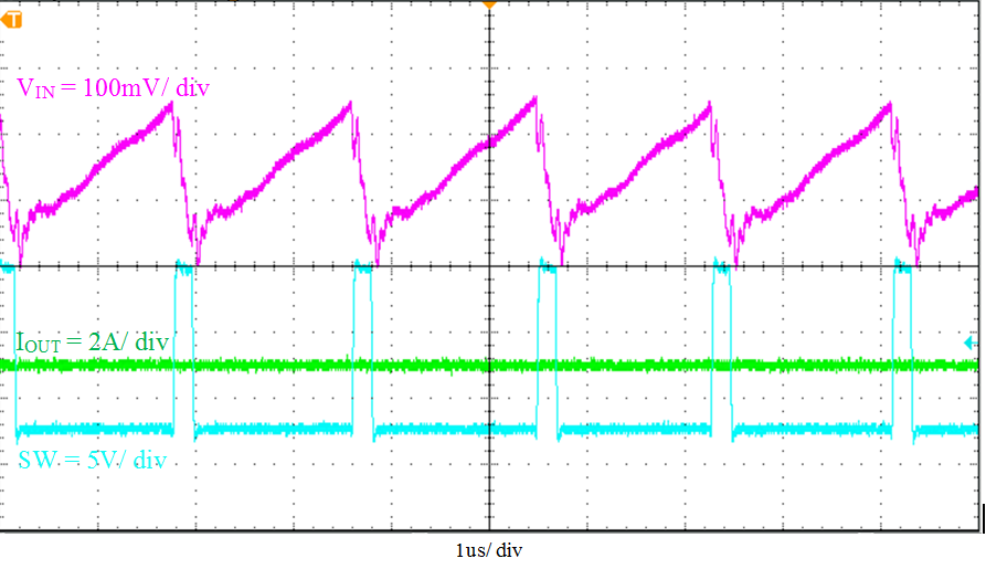
TPS565208 Figure 19. Input Voltage Ripple.png
1 µs/div
Figure 19. TPS565208 Input Voltage Ripple
TPS565208 Output_Voltage_Ripple_IOUT_2p5A_21_SLVSE71.gif
1 µs/div
Figure 21. TPS565208 Output Voltage Ripple, IOUT 2.5 A
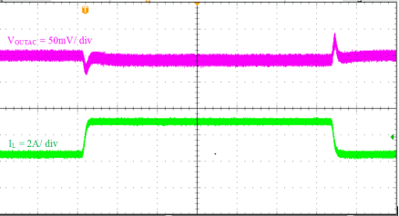
TPS565208 Load_Transient_Response_0p1A_to_2p5A_23_SLVSE72.gif
100 µs/div
Figure 23. TPS565208 Transient Response 0.1 to 2.5 A
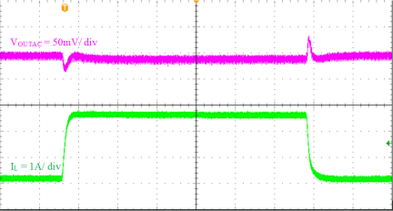
TPS565208 Load_Transient_Response_2p5A_to_5A_25_SLVSE72.gif
100 µs/div
Figure 25. TPS565208 Transient Response, 2.5 to 5 A
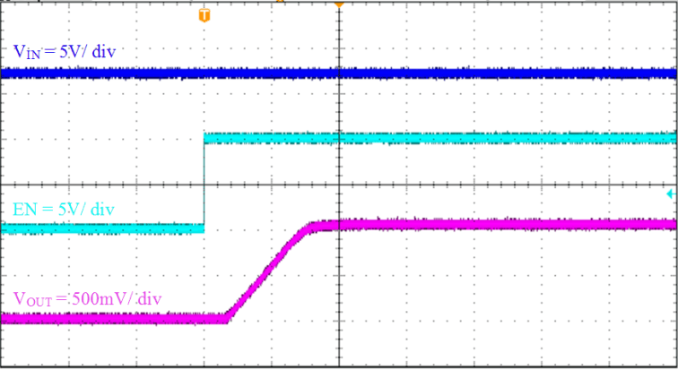
TPS565208 Start-up_Relative_to_EN_27_SLVSE71.gif
400 µs/div
Figure 27. TPS565208 Startup Relative to EN
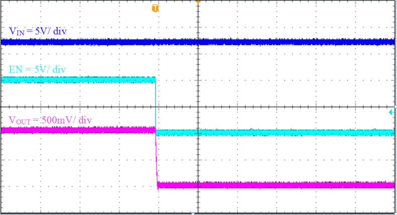
TPS565208 Shut-Down_Relative_to_EN_29_SLVSE71.gif
400 µs/div
Figure 29. TPS565208 Shutdown Relative to EN
TPS565208 D016_SLVSE72.gif
VIN = 12 V VOUT1 = 1.05 V
Figure 16. TPS565208 Load Regulation, VIN = 12 V
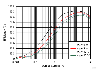
TPS565208 D009_SLVSE72.gif
Figure 18. TPS565208 Efficiency, Vout = 1.05 V
TPS565208 Figure 20. Output Voltage Ripple, no load.png
1 µs/div
Figure 20. TPS565208 Output Voltage Ripple, No Load
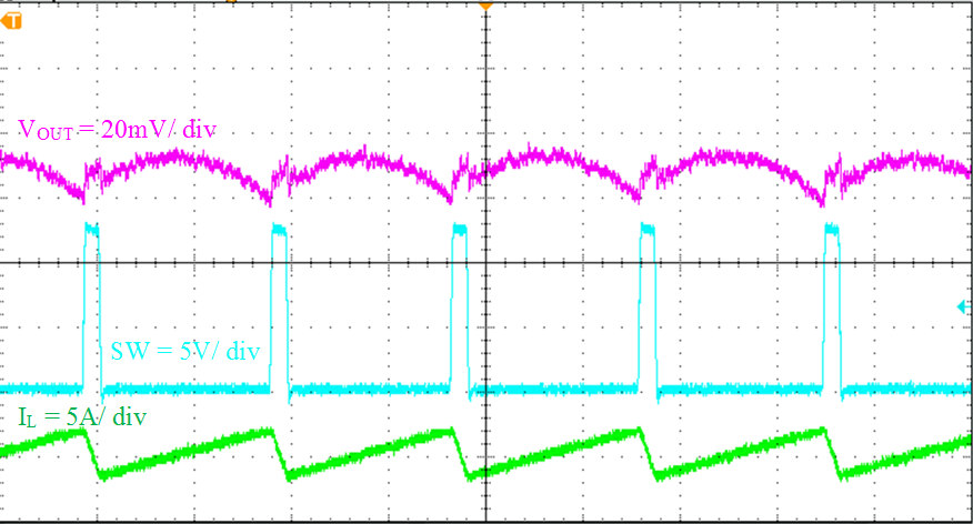
TPS565208 Output_Voltage_Ripple_IOUT_5A_22_SLVSE71.gif
1 µs/div
Figure 22. TPS565208 Output Voltage Ripple, IOUT 5 A
TPS565208 Load_Transient_Response_1p25A_to_3p75A_24_SLVSE71.gif
100 µs/div
Figure 24. TPS565208 Transient Response, 1.25 to 3.75 A
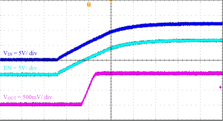
TPS565208 Start-up_Relative_to_VIN_26_SLVSE71.gif
2 ms/div
Figure 26. TPS565208 Startup Relative to VIN
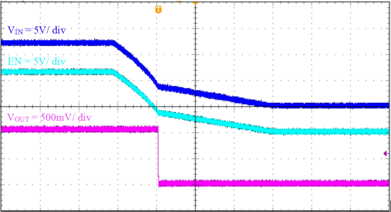
TPS565208 Shut-Down_Relative_to_VIN_28_SLVSE71.gif
20 ms/div
Figure 28. TPS565208 Shutdown Relative to VIN