SLUSDQ7B May   2020  – December 2023 TPS566231 , TPS566238

PRODUCTION DATA  

  1.   1
  2. Features
  3. Applications
  4. Description
  5. Pin Configuration and Functions
  6. Specifications
    1. 5.1 Absolute Maximum Ratings
    2. 5.2 ESD Ratings
    3. 5.3 Recommended Operating Conditions
    4. 5.4 Thermal Information
    5. 5.5 Electrical Characteristics
    6. 5.6 Typical Characteristics
  7. Detailed Description
    1. 6.1 Overview
    2. 6.2 Functional Block Diagram
    3. 6.3 Feature Description
      1. 6.3.1 PWM Operation and D-CAP3™ Control Mode
      2. 6.3.2 Soft Start
      3. 6.3.3 Power Good
      4. 6.3.4 Large Duty Operation
      5. 6.3.5 Overcurrent Protection and Undervoltage Protection
      6. 6.3.6 Overvoltage Protection
      7. 6.3.7 UVLO Protection
      8. 6.3.8 Output Voltage Discharge
      9. 6.3.9 Thermal Shutdown
    4. 6.4 Device Functional Modes
      1. 6.4.1 Advanced Eco-mode Control
      2. 6.4.2 Force CCM Mode
      3. 6.4.3 Standby Operation
  8. Application and Implementation
    1. 7.1 Application Information
    2. 7.2 Typical Application
      1. 7.2.1 Design Requirements
      2. 7.2.2 Detailed Design Procedure
        1. 7.2.2.1 Custom Design with WEBENCH® Tools
        2. 7.2.2.2 Output Voltage Setpoint
        3. 7.2.2.3 Inductor Selection
        4. 7.2.2.4 Output Capacitor Selection
        5. 7.2.2.5 Input Capacitor Selection
      3. 7.2.3 Application Curves
    3. 7.3 Power Supply Recommendations
    4. 7.4 Layout
      1. 7.4.1 Layout Guidelines
      2. 7.4.2 Layout Example
  9. Device and Documentation Support
    1. 8.1 Device Support
      1. 8.1.1 Development Support
        1. 8.1.1.1 Custom Design with WEBENCH® Tools
    2. 8.2 Receiving Notification of Documentation Updates
    3. 8.3 Support Resources
    4. 8.4 Trademarks
    5. 8.5 Electrostatic Discharge Caution
    6. 8.6 Glossary
  10. Revision History
  11. 10Mechanical, Packaging, and Orderable Information

Package Options

Mechanical Data (Package|Pins)
Thermal pad, mechanical data (Package|Pins)
Orderable Information

Input Capacitor Selection

The devices require input decoupling capacitors on power supply input VIN. Also, bulk capacitors are needed depending on the application. The minimum input capacitance required is given in Equation 7.

Equation 7. GUID-48B174DB-414B-4CE9-895F-29A717175277-low.gif

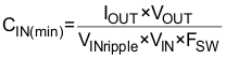
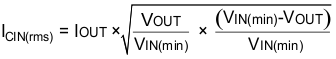
TI recommends using high-quality X5R or X7R input decoupling capacitors of 30 µF on the input voltage pin VIN. The voltage rating on the input capacitor must be greater than the maximum input voltage. The capacitor must also have a ripple current rating greater than the maximum input current ripple of the application. The input ripple current is calculated by Equation 8:

Equation 8. GUID-A5F72520-C517-4237-8470-E4376E9FC717-low.gif

A 1-µF ceramic capacitor is needed for the decoupling capacitor on the VCC pin.