SLVSDI8C
october 2016 – august 2023
TPS568215
PRODUCTION DATA
1
1
Features
2
Applications
3
Description
4
Revision History
5
Pin Configuration and Functions
6
Specifications
6.1
Absolute Maximum Ratings
6.2
ESD Ratings
6.3
Recommended Operating Conditions
6.4
Thermal Information
6.5
Electrical Characteristics
6.6
Timing Requirements
6.7
Typical Characteristics
7
Detailed Description
7.1
Overview
7.2
Functional Block Diagram
7.3
Feature Description
7.3.1
PWM Operation and D-CAP3 Control Mode
7.3.2
Eco-mode Control
7.3.3
4.7 V LDO and External Bias
7.3.4
MODE Selection
7.3.5
Soft Start and Pre-biased Soft Start
7.3.6
Enable and Adjustable UVLO
7.3.7
Power Good
7.3.8
Overcurrent Protection and Undervoltage Protection
7.3.9
Out-of-Bounds Operation
7.3.10
UVLO Protection
7.3.11
Thermal Shutdown
7.3.12
Output Voltage Discharge
7.4
Device Functional Modes
7.4.1
Light Load Operation
7.4.2
Standby Operation
8
Application and Implementation
8.1
Application Information
8.2
Typical Application
8.2.1
Design Requirements
8.2.2
Detailed Design Procedure
8.2.2.1
External Component Selection
8.2.2.1.1
Output Voltage Set Point
8.2.2.1.2
Switching Frequency and Mode Selection
8.2.2.1.3
Inductor Selection
8.2.2.1.4
Output Capacitor Selection
8.2.2.1.5
Input Capacitor Selection
8.2.3
Application Curves
8.3
Power Supply Recommendations
8.4
Layout
8.4.1
Layout Guidelines
8.4.2
Layout Example
9
Device and Documentation Support
9.1
Device Support
9.1.1
Third-Party Products Disclaimer
9.1.2
Development Support
9.2
Receiving Notification of Documentation Updates
9.3
Support Resources
9.4
Trademarks
9.5
Electrostatic Discharge Caution
9.6
Glossary
10
Mechanical, Packaging, and Orderable Information
Package Options
Mechanical Data (Package|Pins)
RNN|18
MPQF456D
Thermal pad, mechanical data (Package|Pins)
Orderable Information
slvsdi8c_oa
slvsdi8c_pm
6.7
Typical Characteristics
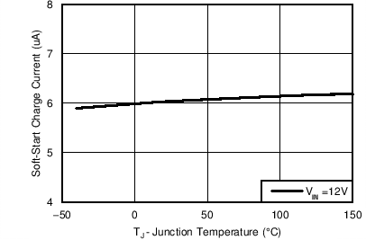
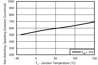
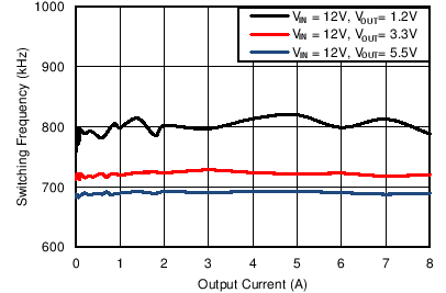
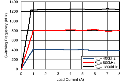
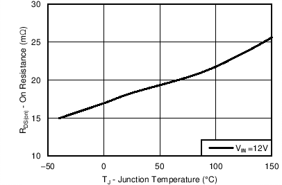
Figure 6-1
Quiescent Current vs Temperature
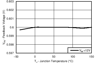
Figure 6-3
Feedback Voltage vs Temperature
Figure 6-5
Low-side R
dson
vs Temperature
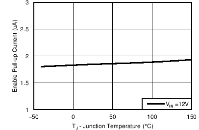
Figure 6-7
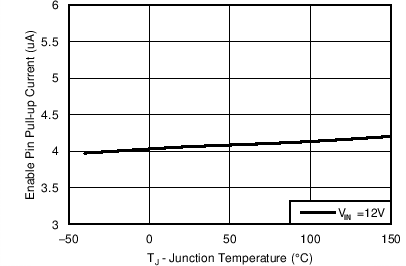
Enable Pull-Up Current, V
EN
=1.0V
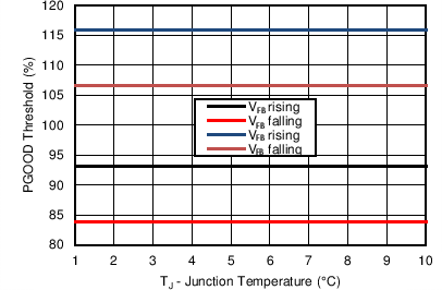
Figure 6-9
PGOOD Threshold vs Temperature
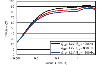
Figure 6-11
Efficiency with Internal VREG5 = 4.7 V, V
IN
= 12 V
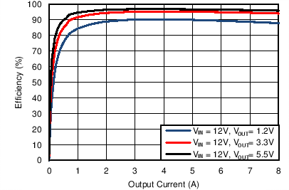
Figure 6-13
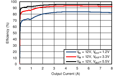
Efficiency, Mode = FCCM, F
SW
= 400kHz
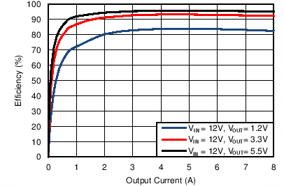
Figure 6-15
Efficiency, Mode = FCCM, F
SW
= 1200kHz
Figure 6-17
F
SW
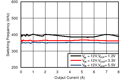
Load Regulation, Mode = FCCM, F
SW
= 400kHz
Figure 6-19
F
SW
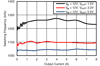
Load Regulation, Mode = FCCM, F
SW
= 1200kHz
Figure 6-2
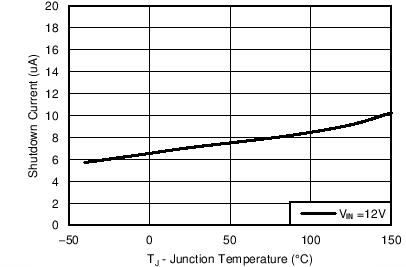
Shutdown Current vs Temperature
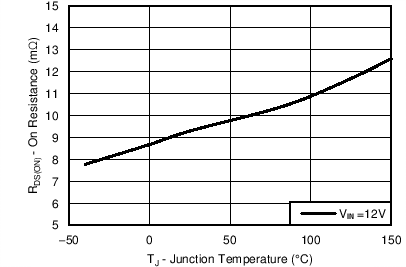
Figure 6-4
High-side R
dson
vs Temperature
Figure 6-6
Soft-Start Charge Current vs Temperature
Figure 6-8
Enable Pull-Up Current, V
EN
=1.3V
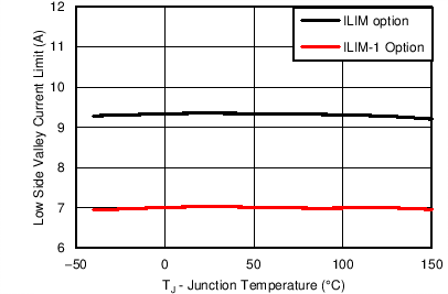
Figure 6-10
Valley Current Limit vs Temperature
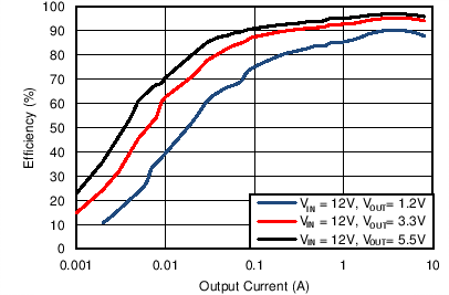
Figure 6-12
Efficiency, Mode = DCM, F
SW
= 400kHz
Figure 6-14
Efficiency, Mode = DCM, F
SW
= 1200kHz
Figure 6-16
Load Regulation, F
SW
= 400kHz
Figure 6-18
F
SW
Load Regulation, Mode = FCCM, F
SW
= 800kHz
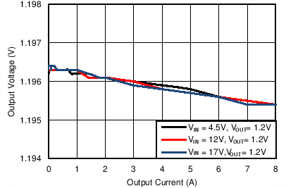
Figure 6-20
F
SW
Load Regulation, Mode = DCM, V
IN
= 12V, V
OUT
=1.2V