SLVSDI8C october 2016 – august 2023 TPS568215
PRODUCTION DATA
- 1
- 1 Features
- 2 Applications
- 3 Description
- 4 Revision History
- 5 Pin Configuration and Functions
- 6 Specifications
-
7 Detailed Description
- 7.1 Overview
- 7.2 Functional Block Diagram
- 7.3
Feature Description
- 7.3.1 PWM Operation and D-CAP3 Control Mode
- 7.3.2 Eco-mode Control
- 7.3.3 4.7 V LDO and External Bias
- 7.3.4 MODE Selection
- 7.3.5 Soft Start and Pre-biased Soft Start
- 7.3.6 Enable and Adjustable UVLO
- 7.3.7 Power Good
- 7.3.8 Overcurrent Protection and Undervoltage Protection
- 7.3.9 Out-of-Bounds Operation
- 7.3.10 UVLO Protection
- 7.3.11 Thermal Shutdown
- 7.3.12 Output Voltage Discharge
- 7.4 Device Functional Modes
- 8 Application and Implementation
- 9 Device and Documentation Support
- 10Mechanical, Packaging, and Orderable Information
Package Options
Mechanical Data (Package|Pins)
- RNN|18
Thermal pad, mechanical data (Package|Pins)
Orderable Information
8.4.2 Layout Example
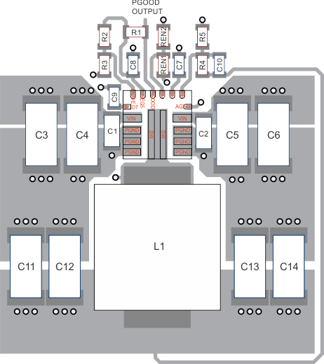
Figure 8-19 shows the recommended top side layout. Component reference designators are the same as the circuit shown in Figure 8-1. Resistor divider for EN is not used in the circuit of Figure 8-1, but are shown in the layout for reference.
 Figure 8-19 Top Side Layout
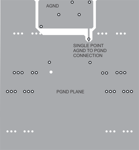
Figure 8-20 shows the recommended layout for the first internal layer. It is comprised of a large PGND plane and a smaller ANGD island. AGND and PGND are connected at a single point to reduce circulating currents.
 Figure 8-20 Mid Layer 1 Layout
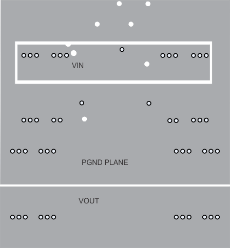
Figure 8-21 shows the recommended layout for the second internal layer. It is comprised of a large PGND plane, a smaller copper fill area to connect the two top side VIN copper areas and a second VOUT copper fill area.
 Figure 8-21 Mid Layer 2 Layout
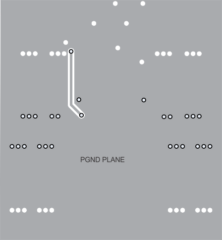
Figure 8-22 shows the recommended layout for the bottom layer. It is comprised of a large PGND plane and a trace to connect the BOOT capacitor to the SW node.
 Figure 8-22 Bottom Layer Layout