SLVSDU5A April 2018 – November 2019 TPS57112C-Q1
PRODUCTION DATA.
- 1 Features
- 2 Applications
- 3 Description
- 4 Revision History
- 5 Pin Configuration and Functions
- 6 Specifications
-
7 Detailed Description
- 7.1 Overview
- 7.2 Functional Block Diagram
- 7.3 Feature Description
- 7.4
Device Functional Modes
- 7.4.1 Adjusting the Output Voltage
- 7.4.2 Enable Functionality and Adjusting Undervoltage Lockout
- 7.4.3 Slow-Start or Tracking Pin
- 7.4.4 Sequencing
- 7.4.5 Constant Switching Frequency and Timing Resistor (RT/CLK Pin)
- 7.4.6 Overcurrent Protection
- 7.4.7 Frequency Shift
- 7.4.8 Reverse Overcurrent Protection
- 7.4.9 Synchronize Using the RT/CLK Pin
- 7.4.10 Power Good (PWRGD Pin)
- 7.4.11 Overvoltage Transient Protection
- 7.4.12 Thermal Shutdown
- 7.4.13 Small-Signal Model for Loop Response
- 7.4.14 Simple Small-Signal Model for Peak-Current-Mode Control
- 7.4.15 Small-Signal Model for Frequency Compensation
-
8 Application and Implementation
- 8.1 Application Information
- 8.2
Typical Application
- 8.2.1 Design Requirements
- 8.2.2
Detailed Design Procedure
- 8.2.2.1 Selecting the Switching Frequency
- 8.2.2.2 Output Inductor Selection
- 8.2.2.3 Output Capacitor
- 8.2.2.4 Input Capacitor
- 8.2.2.5 Slow-Start Capacitor
- 8.2.2.6 Bootstrap Capacitor Selection
- 8.2.2.7 Output Voltage and Feedback Resistor Selection
- 8.2.2.8 Compensation
- 8.2.2.9 Power-Dissipation Estimate
- 8.2.3 Application Curves
- 9 Power Supply Recommendations
- 10Layout
- 11Device and Documentation Support
- 12Mechanical, Packaging, and Orderable Information
Package Options
Mechanical Data (Package|Pins)
- RTE|16
Thermal pad, mechanical data (Package|Pins)
- RTE|16
Orderable Information
7.4.9 Synchronize Using the RT/CLK Pin
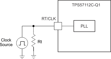
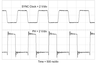
The RT/CLK pin can synchronize the converter to an external system clock. See . To implement the synchronization feature in a system, connect a square wave to the RT/CLK pin with an on-time of at least 75 ns. If the square wave pulls the pin above the PLL upper threshold, a mode change occurs, and the pin becomes a synchronization input. The CLK mode disables the internal amplifier, and the pin is a high-impedance clock input to the internal PLL. Stopping the clocking edges re-enables the internal amplifier, and the mode returns to the frequency set by the resistor. The square-wave amplitude at this pin must transition lower than 0.6 V and higher than 1.6 V, typically. The synchronization frequency range is 300 kHz to 2000 kHz. The rising edge of PH synchronizes to the falling edge of the RT/CLK pin.
 Figure 29. Synchronizing to a System Clock
  Figure 30. Plot of Synchronizing to System Clock