SLVSDQ7B October 2016 – July 2021 TPS57114C-Q1
PRODUCTION DATA
- 1 Features
- 2 Applications
- 3 Description
- 4 Revision History
- 5 Pin Configuration and Functions
- 6 Specifications
-
7 Detailed Description
- 7.1 Overview
- 7.2 Functional Block Diagram
- 7.3 Feature Description
- 7.4
Device Functional Modes
- 7.4.1 Adjusting the Output Voltage
- 7.4.2 Enable Functionality and Adjusting Undervoltage Lockout
- 7.4.3 Slow-Start or Tracking Pin
- 7.4.4 Sequencing
- 7.4.5 Constant Switching Frequency and Timing Resistor (RT/CLK Pin)
- 7.4.6 Overcurrent Protection
- 7.4.7 Frequency Shift
- 7.4.8 Reverse Overcurrent Protection
- 7.4.9 Synchronize Using The RT/CLK Pin
- 7.4.10 Power Good (PWRGD Pin)
- 7.4.11 Overvoltage Transient Protection
- 7.4.12 Thermal Shutdown
- 7.4.13 Small-Signal Model for Loop Response
- 7.4.14 Simple Small-Signal Model for Peak-Current Mode Control
- 7.4.15 Small-Signal Model for Frequency Compensation
-
8 Application and Implementation
- 8.1 Application Information
- 8.2
Typical Application
- 8.2.1 Design Requirements
- 8.2.2
Detailed Design Procedure
- 8.2.2.1 Selecting the Switching Frequency
- 8.2.2.2 Output Inductor Selection
- 8.2.2.3 Output Capacitor
- 8.2.2.4 Input Capacitor
- 8.2.2.5 Slow-Start Capacitor
- 8.2.2.6 Bootstrap Capacitor Selection
- 8.2.2.7 Output-Voltage And Feedback-Resistor Selection
- 8.2.2.8 Compensation
- 8.2.2.9 Power-Dissipation Estimate
- 8.2.3 Application Curves
- 9 Power Supply Recommendations
- 10Layout
- 11Device and Documentation Support
- 12Mechanical, Packaging, and Orderable Information
Package Options
Mechanical Data (Package|Pins)
- RTE|16
Thermal pad, mechanical data (Package|Pins)
- RTE|16
Orderable Information
8.2.2.7 Output-Voltage And Feedback-Resistor Selection
For the example design, the selection for R6 is 100 kΩ. Using Equation 33, calculate R7 as 80 kΩ. The nearest standard 1% resistor is 80.5 kΩ.
Equation 33. 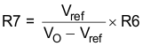
Due to the internal design of the TPS57114C-Q1 device, there is a minimum output voltage limit for any given input voltage. The output voltage can never be lower than the internal voltage reference of 0.8 V. Above 0.8 V, an output voltage limit may exist due to the minimum controllable on-time. In this case, Equation 34 gives the minimum output voltage
Equation 34. 
where
- VO(min) = minimum achievable output voltage
- t(ONmin) = minimum controllable on-time (65 ns, typical; 120 ns, no load)
- f(SWmax) = maximum switching frequency, including tolerance
- VI(max) = maximum input voltage
- IO(min) = minimum load current
- rDS(on) = minimum high-side MOSFET on-resistance (15 mΩ–19 mΩ)
- R(L) = series resistance of output inductor
There is also a maximum achievable output voltage, which is limited by the minimum off-time. Equation 35 gives the maximum output voltage.
Equation 35. 
where
- VO(max) = maximum achievable output voltage
- t(OFFmax) = maximum off-time (60 ns, typical)
- f(SWmax) = maximum switching frequency, including tolerance
- VI(min) = minimum input voltage
- IO(max) = maximum load current
- rDS(on) = maximum high-side MOSFET on-resistance (19 mΩ–30 mΩ)
- R(L) = series resistance of output inductor